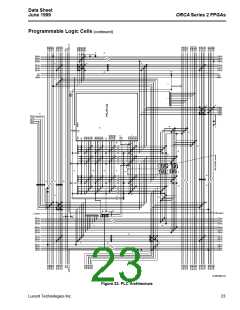
Data Sheet
June 1999
ORCA Series 2 FPGAs
the input buffer characteristics of the other device when
driven at the OR2TxxB output buffer voltage levels.
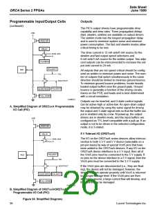
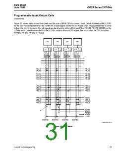
Programmable Input/Output Cells
(continued)
The OR2TxxB device has internal programmable pull-
ups on the I/O buffers. These pull-up voltages are
always referenced to VDD and are always sufficient to
pull the input buffer of the OR2TxxB device to a high
state. The pin on the OR2TxxB device will be at a level
1.0 V below VDD (minimum of 2.0 V with a minimum
VDD of 3.0 V). This voltage is sufficient to pull the exter-
nal pin up to a 3.3 V CMOS high-input level (1.8 V, min)
or a TTL high input level (2.0 V, min) in a 5 V tolerant
system. Therefore, in a 5 V tolerant system using 5 V
CMOS parts, care must be taken to evaluate the use of
these pull-ups to pull the pin of the OR2TxxB device to
a typical 5 V CMOS high-input level (2.2 V, min).
Regardless of the power supply that the VDD5 pins are
connected to (5 V or 3.3 V), the OR2TxxA devices will
drive the pin to the 3.3 V levels when the output buffer
is enabled. If the other device being driven by the
OR2TxxA device has TTL-compatible inputs, then the
device will not dissipate much input buffer power. This
is because the OR2TxxA output is being driven to a
higher level than the TTL level required. If the other
device has a CMOS-compatible input, the amount of
input buffer power will also be small. Both of these
power values are dependent upon the input buffer char-
acteristics of the other device when driven at the
OR2TxxA output buffer voltage levels.
The 2TxxA device has internal programmable pull-ups
on the I/O buffers. These pull-up voltages are always
referenced to VDD. This means that the VDD5 voltage
has no effect on the value of the pull-up voltage at the
pad. This voltage level is always sufficient to pull the
input buffer of the 2TxxA device to a high state. The pin
on the 2TxxA device will be at a level 1.0 V below VDD
(minimum of 2.0 V with a minimum VDD of 3.0 V). This
voltage is sufficient to pull the external pin up to a 3.3 V
CMOS high-input level (1.8 V min) or a TTL high-input
level (2.0 V min) in a 5 V tolerant system, but it will
never pull the pad up to the VDD5 rail. Therefore, in a
5 V tolerant system using 5 V CMOS parts, care must
be taken to evaluate the use of these pull-ups to pull
the pin of the 2TxxA device to a typical 5 V CMOS
high-input level (2.2 V min).
PCI Compliant I/O
The I/O on the OR2TxxB Series devices allows compli-
ance with PCI local bus (Rev. 2.1) 5 V and 3.3 V signal-
ing environments. The signaling environment used for
each input buffer can be selected on a per-pin basis.
The selection provides the appropriate I/O clamping
diodes for PCI compliance.
OR2TxxB devices have 5 V tolerant I/Os as previously
explained, but can optionally be selected on a pin-by-
pin basis to be PCI bus 3.3 V signaling compliant (PCI
bus 5 V signaling compliance occurs in 5 V tolerant
operation mode). Inputs may have a pull-up or pull-
down resistor selected on an input for signal stabiliza-
tion and power management. Input signals in a PIO
can be passed to PIC routing on any of three paths,
two general signal paths into PIC routing, and/or a fast
route into the clock routing system.
For more information on 5 V tolerant I/Os, please see
ORCA® Series 5 V Tolerant I/Os Application Note
(AP99-027FPGA), May 1999.
OR2TxxA series devices are only compliant in 3.3 V
PCI Local Bus (Rev 2.1) signalling environments.
OR2CxxA devices are only compliant in 5 V PCI Local
Bus (Rev 2.1) signalling environments.
5 V Tolerant I/O (OR2TxxB)
The I/O on the OR2TxxB Series devices allow intercon-
nection to both 3.3 V and 5 V device (selectable on a
per-pin basis). Unlike the OR2TxxA family, when inter-
faceing into a 5 V signal, it no longer requires a VDD5
supply.
The OR2TxxB devices will drive the pin to the 3.3 V lev-
els when the output buffer is enabled. If the other
device being driven by the OR2TxxB device has TTL-
compatible inputs, then the device will not dissipate
much input buffer power. This is because the OR2TxxB
output is being driven to a higher level than the TTL
level required. If the other device has a CMOS-compat-
ible input, the amount of input buffer power will also be
small. Both of these power values are dependent upon
Lucent Technologies Inc.
27

 ETC [ ETC ]