Data Sheet
June 1999
ORCA Series 2 FPGAs
Programmable Input/Output Cells
(continued)
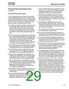
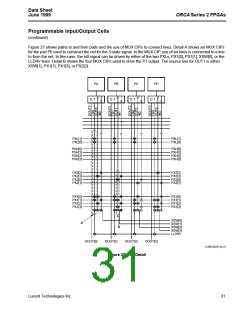
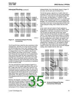
Figure 27 shows paths to and from pads and the use of MUX CIPs to connect lines. Detail A shows six MUX CIPs
for the pad P0 used to construct the net for the 3-state signal. In the MUX CIP, one of six lines is connected to a line
to form the net. In this case, the ts0 signal can be driven by either of the two PXLs, PX1[0], PX1[1], XSW[0], or the
LLDRV lines. Detail B shows the four MUX CIPs used to drive the P1 output. The source line for OUT1 is either
XSW[1], PX1[1], PX1[3], or PX2[2].
PA
PB
PC
PD
D T
D T
D T
D T
PXL[1]
PXL[0]
PXL[1]
PXL[0]
PXH[0]
PXH[1]
PXH[2]
PXH[3]
PXH[0]
PXH[1]
PXH[2]
PXH[3]
PX2[2]
PX2[3]
PX2[0]
PX2[1]
PX2[2]
PX2[3]
PX2[0]
PX2[1]
PX1[0]
PX1[1]
PX1[2]
PX1[3]
PX1[0]
PX1[1]
PX1[2]
PX1[3]
XSW[0]
XSW[1]
XSW[2]
XSW[3]
LLDRV
A
B
DOUT[0]
DOUT[1]
DOUT[2]
DOUT[3]
5-2843.BL(F).2C.r3
Figure 27. PIC Detail
Lucent Technologies Inc.
31

 ETC [ ETC ]