Data Sheet
June 1999
ORCA Series 2 FPGAs
sides are left (L), right (R), top (T), and bottom (B). The
individual I/O pad is indicated by a single letter (either
A, B, C, or D) placed at the end of the PIC name. As an
example, PL10A indicates a pad located on the left
side of the array in the tenth row.
Programmable Input/Output Cells
(continued)
PIC Routing Resources
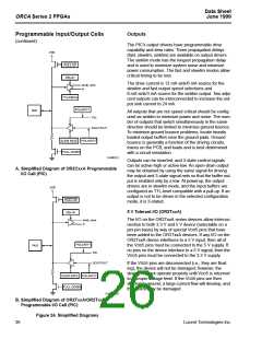
Each PIC has four pads and each pad can be config-
ured as an input, an output (3-statable), a direct output,
or a bidirectional I/O. When the pads are used as
inputs, the external signals are provided to the internal
circuitry at IN[3:0]. When the pads are used to provide
direct inputs to the latches/FFs, they are connected
through DIN[3:0]. When the pads are used as outputs,
the internal signals connect to the pads through
OUT[3:0]. When the pads are used as direct outputs,
the output from the latches/flip-flops in the PLCs to the
PIC is designated DOUT[3:0]. When the outputs are
3-statable, the 3-state enable signals are TS[3:0].
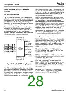
The PIC routing is designed to route 4-bit wide buses
efficiently. For example, any four consecutive I/O pads
can have both their input and output signals routed into
one PLC. Using only PIC routing, either the input or
output data can be routed to/from a single PLC from/to
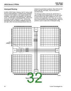
any eight pads in a row, as in Figure 25.
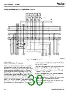
The connections between PLCs and the I/O pad are
provided by two basic types of routing resources.
These are routing resources internal to the PIC and
routing resources used for PIC-PLC connection.
Figure 26 and Figure 27 show a high-level and detailed
view of these routing resources, respectively.
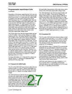
Routing Resources Internal to the PIC
PXL PXH PX2 PX1
For inter-PIC routing, the PIC contains 14 lines used to
route signals around the perimeter of the FPGA. Figure
25 shows these lines running vertically for a PIC
located on the left side. Figure 26 shows the lines run-
ning horizontally for a PIC located at the top of the
FPGA.
2
4
4
4
2
4
4
5
4
4
4
4
4
4
CK
PLC X4
PLC X1
PLC PSW
PLC DOUT
PLC XL
PLC XH
PLC X1
PLC X4
PLC DIN
4
4
4
4
PAD D
PAD C
PAD B
PAD A
I/O3
I/O2
I/O1
I/O0
PIC
SWITCHING
MATRIX
PXL Lines. Each PIC has two PXL lines, labeled
PXL[1:0]. Like the XL lines of the PLC, the PXL lines
span the entire edge of the FPGA.
PXH Lines. Each PIC has four PXH lines, labeled
PXH[3:0]. Like the XH lines of the PLC, the PXH lines
span half the edge of the FPGA.
2
4
4
4
PXL PXH PX2 PX1
PX2 Lines. There are four PX2 lines in each PIC,
labeled PX2[3:0]. The PX2 lines pass through two adja-
cent PICs before being broken. These are used to
route nets around the perimeter equally a distance of
two or more PICs.
5-4504(F)
Figure 25. Simplified PIC Routing Diagram
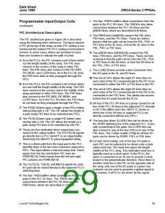
The PIC’s name is represented by a two-letter designa-
tion to indicate on which side of the device it is located
followed by a number to indicate in which row or col-
umn it is located. The first letter, P, designates that the
cell is a PIC and not a PLC. The second letter indicates
the side of the array where the PIC is located. The four
PX1 Lines. Each PIC has four PX1 lines, labeled
PX1[3:0]. The PX1 lines are one PIC long and are
extended to adjacent PICs by enabling CIPs.
28
Lucent Technologies Inc.

 ETC [ ETC ]