Data Sheet
June 1999
ORCA Series 2 FPGAs
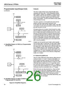
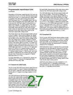
Outputs
Programmable Input/Output Cells
(continued)
The PIC’s output drivers have programmable drive
capability and slew rates. Three propagation delays
(fast, slewlim, sinklim) are available on output drivers.
The sinklim mode has the longest propagation delay
and is used to minimize system noise and minimize
power consumption. The fast and slewlim modes allow
critical timing to be met.
VDD
PULL-UP
DELAY
The drive current is 12 mA sink/6 mA source for the
slewlim and fast output speed selections and
6 mA sink/3 mA source for the sinklim output. Two adja-
cent outputs can be interconnected to increase the out-
put sink current to 24 mA.
dintb, dinlr
in
TTL/CMOS
POLARITY
PAD
All outputs that are not speed critical should be config-
ured as sinklim to minimize power and noise. The num-
ber of outputs that switch simultaneously in the same
direction should be limited to minimize ground bounce.
To minimize ground bounce problems, locate heavily
loaded output buffers near the ground pads. Ground
bounce is generally a function of the driving circuits,
traces on the PCB, and loads and is best determined
with a circuit simulation.
TRI
DOUT/OUT
SLEW RATE
POLARITY
PULL-DOWN
5-4591(F)
Outputs can be inverted, and 3-state control signals
can be active-high or active-low. An open-drain output
may be obtained by using the same signal for driving
the output and 3-state signal nets so that the buffer out-
put is enabled only by a low. At powerup, the output
drivers are in slewlim mode, and the input buffers are
configured as TTL-level compatible with a pull-up. If an
output is not to be driven in the selected configuration
mode, it is 3-stated.
A. Simplified Diagram of OR2CxxA Programmable
I/O Cell (PIC)
VDD
PULL-UP
DELAY
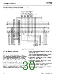
5 V Tolerant I/O (OR2TxxA)
The I/O on the OR2TxxA series devices allow intercon-
nection to both 3.3 V and 5 V device (selectable on a
per-pin basis) by way of special VDD5 pins that have
been added to the OR2TxxA devices. If any I/O on the
OR2TxxA device interfaces to a 5 V input, then all of
the VDD5 pins must be connected to the 5 V supply. If
no pins on the device interface to a 5 V signal, then the
VDD5 pins must be connected to the 3.3 V supply.
dintb, dinlr
in
POLARITY
PAD
TRI
DOUT/OUT
If the VDD5 pins are disconnected (i.e., they are float-
ing), the device will not be damaged; however, the
device may not operate properly until VDD5 is returned
to a proper voltage level. If the VDD5 pins are then
shorted to ground, a large current flow will develop, and
the device may be damaged.
SLEW RATE POLARITY
PULL-DOWN
5-4591.T(F)
B. Simplified Diagram of OR2TxxA/OR2TxxB
Programmable I/O Cell (PIC)
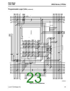
Figure 24. Simplified Diagrams
26
Lucent Technologies Inc.

 ETC [ ETC ]