Data Sheet
June 1999
ORCA Series 2 FPGAs
Inputs
Programmable Input/Output Cells
Each I/O can be configured to be either an input, an
output, or bidirectional I/O. Inputs for the OR2CxxA can
be configured as either TTL or CMOS compatible. The
I/O for the OR2TxxA and OR2TxxB series devices are
5 V tolerant, and will be described in a later section of
this data sheet. Pull-up or pull-down resistors are avail-
able on inputs to minimize power consumption.
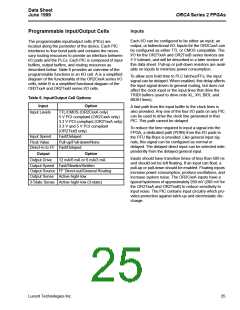
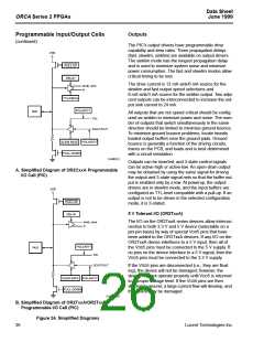
The programmable input/output cells (PICs) are
located along the perimeter of the device. Each PIC
interfaces to four bond pads and contains the neces-
sary routing resources to provide an interface between
I/O pads and the PLCs. Each PIC is composed of input
buffers, output buffers, and routing resources as
described below. Table 6 provides an overview of the
programmable functions in an I/O cell. A is a simplified
diagram of the functionality of the OR2CxxA series I/O
cells, while B is a simplified functional diagram of the
OR2TxxA and OR2TxxB series I/O cells.
To allow zero hold time to PLC latches/FFs, the input
signal can be delayed. When enabled, this delay affects
the input signal driven to general routing, but does not
affect the clock input or the input lines that drive the
TRIDI buffers (used to drive onto XL, XH, BIDI, and
BIDIH lines).
Table 6. Input/Output Cell Options
Input
Option
A fast path from the input buffer to the clock lines is
also provided. Any one of the four I/O pads on any PIC
can be used to drive the clock line generated in that
PIC. This path cannot be delayed.
Input Levels
TTL/CMOS (OR2CxxA only)
5 V PCI compliant (OR2CxxA only)
3.3 V PCI compliant (OR2TxxA only)
3.3 V and 5 V PCI compliant
(OR2TxxB only)
To reduce the time required to input a signal into the
FPGA, a dedicated path (PDIN) from the I/O pads to
the PFU flip-flops is provided. Like general input sig-
nals, this signal can be configured as normal or
delayed. The delayed direct input can be selected inde-
pendently from the delayed general input.
Input Speed
Float Value
Fast/Delayed
Pull-up/Pull-down/None
Direct-in to FF Fast/Delayed
Output
Option
12 mA/6 mA or 6 mA/3 mA
Inputs should have transition times of less than 500 ns
and should not be left floating. If an input can float, a
pull-up or pull-down should be enabled. Floating inputs
increase power consumption, produce oscillations, and
increase system noise. The OR2CxxA inputs have a
typical hysteresis of approximately 280 mV (200 mV for
the OR2TxxA and OR2TxxB) to reduce sensitivity to
input noise. The PIC contains input circuitry which pro-
vides protection against latch-up and electrostatic dis-
charge.
Output Drive
Output Speed Fast/Slewlim/Sinklim
Output Source FF Direct-out/General Routing
Output Sense Active-high/-low
3-State Sense Active-high/-low (3-state)
Lucent Technologies Inc.
25

 ETC [ ETC ]