Proprietary TranSwitch Corporation Information for use Solely by its Customers
L3M
TXC-03452B
DATA SHEET
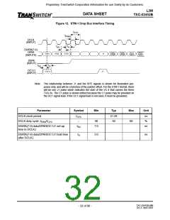
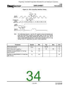
Figure 14. STS-1 Drop Bus Interface Timing
tCYC
tPWH
DCLK
(INPUT)
tH
tSU
DDATA(7-0)
DPAR
(INPUTS)
C1
DATA
DATA
J1
DATA
DATA
DATA
DSPE
(INPUT)
tSU
tH
DC1J1
(INPUT)
C1
J1
Note: The relationship between J1 and the SPE signals is shown for illustration pur-
poses only, and will be a function of the pointer offset. For the STS-1 format,
there will be one J1 pulse which indicates the start of the STS-1 SPE. The C1
pulse is shown dotted because the C1 pulse may be provided on the DC1 sig-
nal lead. If the DC1 signal lead is not used, it must be grounded.
Parameter
DCLK clock period
Symbol
Min
Typ
Max
Unit
tCYC
--
154.32
50
ns
%
DCLK duty cycle, tPWH/tCYC
40
60
DDATA(7-0) data/DPAR/DC1J1 set-up
tSU
7.0
ns
time to DCLK↓
DDATA(7-0) data/DPAR/DC1J1 hold time
tH
3.0
ns
after DCLK↓
TXC-03452B-MB
Ed. 6, April 2001
- 34 of 96 -

 ETC [ ETC ]