Proprietary TranSwitch Corporation Information for use Solely by its Customers
L3M
TXC-03452B
DATA SHEET
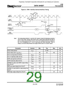
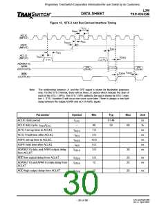
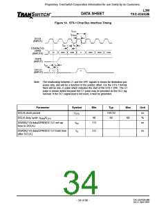
Figure 10. STS-3 Add Bus Derived Interface Timing
tCYC
tPWH
ACLK
(INPUT)
tH(2)
tSU(2)
ASPE
(INPUT)
tOD(1)
tH(1)
AC1J1
(INPUT)
tSU(1)
tOD(3)
J1 for
STS-1 #1
C1(1)
ADATA(7-0)
APAR
(OUTPUTS)
DATA
STS-1#1
DATA
STS-1#1
J1 STS1#1
tOD(2)
tOD(4)
ADD
(OUTPUT)
Note: The relationship between J1 and the SPE signal is shown for illustration purposes
only. For the STS-3 format, there will be three J1 pulses which indicate the start of
each of the STS-1 SPEs. The STS-1 SPE added to the bus is shown for STS-1 num-
ber 1. STS-1 number 2 will occur one clock cycle later. There is always a one byte
delay between the output ADATA and AC1J1/ASPE inputs.
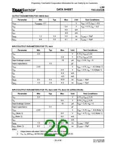
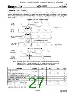
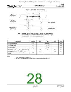
Parameter
ACLK clock period
Symbol
Min
Typ
Max
Unit
tCYC
--
51.44
50
ns
%
ACLK duty cycle, tPWH/tCYC
AC1J1 set-up time to ACLK↓
AC1J1 hold time after ACLK↓
ASPE set-up time to ACLK↓
ASPE hold time after ACLK↓
40
7.0
3.0
10.0
5.0
3.0
60
tSU(1)
tH(1)
tSU(2)
tH(2)
tOD(1)
ns
ns
ns
ns
ns
ADATA(7-0) data and APAR output delay
30
from ACLK↑
ADD low output delay from ACLK↑
tOD(2)
tOD(3)
3.0
12
25
25
ns
ns
ADATA(7-0) and APAR tri-state delay from
ACLK↑
ADD high output delay from ACLK↑
tOD(4)
12
25
ns
TXC-03452B-MB
Ed. 6, April 2001
- 30 of 96 -

 ETC [ ETC ]