Proprietary TranSwitch Corporation Information for use Solely by its Customers
L3M
TXC-03452B
DATA SHEET
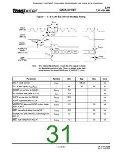
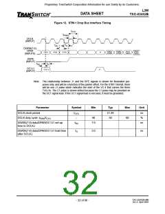
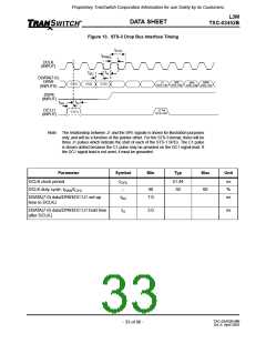
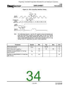
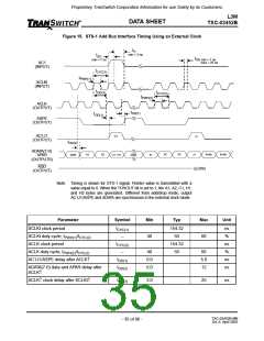
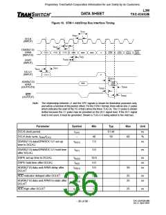
Figure 12. STM-1 Drop Bus Interface Timing
tCYC
tPWH
DCLK
(INPUT)
tH
tSU
DDATA(7-0)
DPAR
(INPUTS)
FIXED
STUFF
FIXED
STUFF
H1(1)
TUG-3
H1(2)
TUG-3
C1(1)
C1(2)
C1(3)
J1
DSPE
(INPUT)
tSU
tH
DC1J1
(INPUT)
C1(1)
J1
Note: The relationship between J1 and the SPE signals is shown for illustration pur-
poses only, and will be a function of the pointer offset. For the STM-1 format, there
will be one J1 pulse which indicates the start of the VC-4 that carries the three
TUG-3s. The C1 pulse is shown dotted because the C1 pulse may be provided on
the DC1 signal lead. If the DC1 signal lead is not used, it must be grounded.
Parameter
DCLK clock period
Symbol
Min
Typ
Max
Unit
tCYC
--
51.44
50
ns
%
DCLK duty cycle, tPWH/tCYC
40
60
DDATA(7-0) data/DPAR/DC1J1 set-up
tSU
7.0
ns
time to DCLK↓
DDATA(7-0) data/DPAR/DC1J1 hold time
tH
3.0
ns
after DCLK↓
TXC-03452B-MB
Ed. 6, April 2001
- 32 of 96 -

 ETC [ ETC ]