Proprietary TranSwitch Corporation Information for use Solely by its Customers
L3M
TXC-03452B
DATA SHEET
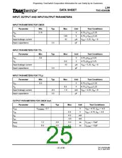
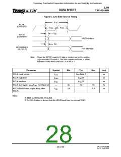
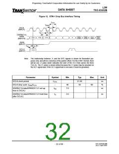
Figure 8. Line Side Receive Timing
tCYC
RCLK
(OUTPUT)
tPWL
tPWH
tOD
RPOS
(OUTPUT)
NRZ Interface
Rail Interface
tOD
RPOS/RNEG
(OUTPUT)
Note: Shown for INVCO equal to 0; data is clocked out on the positive
edge when INVCO equals 1. The three signals are forced to a high
impedance state when control bit L3Z is set to 1.
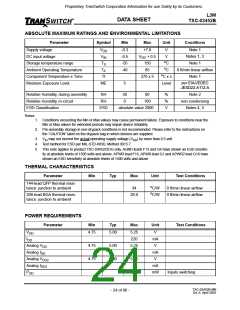
Parameter
Symbol
Min
Typ
Max
Unit
RCLK clock period
tCYC
tPWH
tPWL
---
See Note 1
tCYC/2
tCYC/2
50
ns
ns
ns
%
RCLK high time
RCLK low time
RCLK duty cycle, tPWH/tCYC (See Note 2)
45
55
RPOS/RNEG data output delay after
tOD
-2.0
5.0
ns
RCLK↓
Notes:
1. 22.35 ns (DS3) or 29.10 ns (E3).
2. The RCLK output is derived from the XOSCI input from the external VCXO.
TXC-03452B-MB
Ed. 6, April 2001
- 28 of 96 -

 ETC [ ETC ]