APEX 20K Programmable Logic Device Family Data Sheet
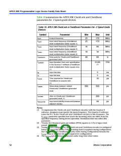
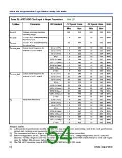
Table 18. APEX 20KE Clock Input & Output Parameters
Note (1)
Symbol
Parameter
I/O Standard
-1X Speed Grade
-2X Speed Grade Units
Min
Max
Min
Max
fVCO (4)
Voltage controlled oscillator
operating range
200
500
200
500
MHz
MHz
MHz
fCLOCK0
Clock0PLL output frequency
1.5
20
335
335
1.5
20
200
200
for internal use
fCLOCK1
Clock1PLL output frequency
for internal use
fCLOCK0_EXT
Output clock frequency for
3.3-V LVTTL
2.5-V LVTTL
1.8-V LVTTL
GTL+
1.5
1.5
1.5
1.5
1.5
1.5
1.5
1.5
1.5
20
245
234
223
205
158
142
166
149
420
245
234
223
205
158
142
166
149
420
290
281
272
303
291
291
300
300
420
1.5
1.5
1.5
1.5
1.5
1.5
1.5
1.5
1.5
20
226
221
216
193
157
142
162
146
350
226
221
216
193
157
142
162
146
350
257
250
243
261
253
253
260
260
350
MHz
MHz
MHz
MHz
MHz
MHz
MHz
MHz
MHz
MHz
MHz
MHz
MHz
MHz
MHz
MHz
MHz
MHz
MHz
MHz
MHz
MHz
MHz
MHz
MHz
MHz
MHz
external clock0output
SSTL-2 Class I
SSTL-2 Class II
SSTL-3 Class I
SSTL-3 Class II
LVDS
fCLOCK1_EXT
Output clock frequency for
3.3-V LVTTL
2.5-V LVTTL
1.8-V LVTTL
GTL+
external clock1output
20
20
20
20
20
20
SSTL-2 Class I
SSTL-2 Class II
SSTL-3 Class I
SSTL-3 Class II
LVDS
20
20
20
20
20
20
20
20
20
20
fIN
Input clock frequency
3.3-V LVTTL
2.5-V LVTTL
1.8-V LVTTL
GTL+
1.5
1.5
1.5
1.5
1.5
1.5
1.5
1.5
1.5
1.5
1.5
1.5
1.5
1.5
1.5
1.5
1.5
1.5
SSTL-2 Class I
SSTL-2 Class II
SSTL-3 Class I
SSTL-3 Class II
LVDS
Notes to tables:
(1) All input clock specifications must be met. The PLL may not lock onto an incoming clock if the clock specifications
are not met, creating an erroneous clock within the device.
(2) The maximum lock time is 40 µs or 2000 input clock cycles, whichever occurs first.
(3) Before configuration, the PLL circuits are disable and powered down. During configuration, the PLLs are still
disabled. The PLLs begin to lock once the device is in the user mode. If the clock enable feature is used, lock begins
once the CLKLK_ENApin goes high in user mode.
(4) The PLL VCO operating range is 200 MHz ð f
ð 840 MHz for LVDS mode.
VCO
54
Altera Corporation

 ETC [ ETC ]