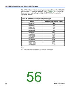
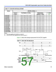
APEX 20K Programmable Logic Device Family Data Sheet
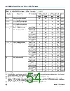
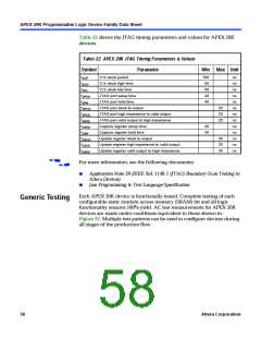
Table 22 shows the JTAG timing parameters and values for APEX 20K
devices.
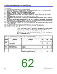
Table 22. APEX 20K JTAG Timing Parameters & Values
Symbol
Parameter
Min Max Unit
tJCP
TCKclock period
100
50
50
20
45
ns
ns
ns
ns
ns
ns
ns
ns
ns
ns
ns
ns
ns
tJCH
TCKclock high time
TCKclock low time
JTAG port setup time
JTAG port hold time
tJCL
tJPSU
tJPH
tJPCO
tJPZX
tJPXZ
tJSSU
tJSH
JTAG port clock to output
25
25
25
JTAG port high impedance to valid output
JTAG port valid output to high impedance
Capture register setup time
20
45
Capture register hold time
tJSCO
tJSZX
tJSXZ
Update register clock to output
35
35
35
Update register high impedance to valid output
Update register valid output to high impedance
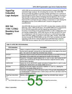
For more information, see the following documents:
f
ꢀ
ꢀ
Application Note 39 (IEEE Std. 1149.1 (JTAG) Boundary-Scan Testing in
Altera Devices)
Jam Programming & Test Language Specification
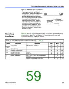
Each APEX 20K device is functionally tested. Complete testing of each
configurable static random access memory (SRAM) bit and all logic
functionality ensures 100% yield. AC test measurements for APEX 20K
devices are made under conditions equivalent to those shown in
Figure 32. Multiple test patterns can be used to configure devices during
all stages of the production flow.
Generic Testing
58
Altera Corporation

 ETC [ ETC ]