APEX 20K Programmable Logic Device Family Data Sheet
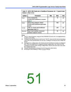
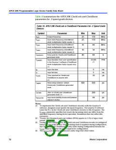
Table 16 summarizes the APEX 20K ClockLock and ClockBoost
parameters for -2 speed grade devices.
Table 16. APEX 20K ClockLock & ClockBoost Parameters for -2 Speed Grade
Devices
Symbol
Parameter
Min
Max
Unit
fOUT
Output frequency
25
25
170
170
MHz
MHz
fCLK1
Input clock frequency (ClockBoost
clock multiplication factor equals 1)
fCLK2
Input clock frequency (ClockBoost
clock multiplication factor equals 2)
16
10
40
80
34
60
MHz
MHz
%
fCLK4
Input clock frequency (ClockBoost
clock multiplication factor equals 4)
tOUTDUTY
fCLKDEV
Duty cycle for ClockLock/ClockBoost-
generated clock
Input deviation from user specification
in the Quartus II software (ClockBoost
clock multiplication factor equals one)
(1)
25,000
(2)
PPM
tR
Input rise time
Input fall time
5
5
ns
ns
µs
tF
tLOCK
Time required for ClockLock/
ClockBoost to acquire lock
(3)
10
tSKEW
Skew delay between related
ClockLock/ ClockBoost-generated
clock
500
500
ps
tJITTER
Jitter on ClockLock/ ClockBoost-
200
50
ps
ps
generated clock (4)
tINCLKSTB
Input clock stability (measured between
adjacent clocks)
Notes:
(1) To implement the ClockLock and ClockBoost circuitry with the Quartus II
software, designers must specify the input frequency. The Quartus II software
tunes the PLL in the ClockLock and ClockBoost circuitry to this frequency. The
f
parameter specifies how much the incoming clock can differ from the
CLKDEV
specified frequency during device operation. Simulation does not reflect this
parameter.
(2) Twenty-five thousand parts per million (PPM) equates to 2.5% of input clock
period.
(3) During device configuration, the ClockLock and ClockBoost circuitry is configured
before the rest of the device. If the incoming clock is supplied during configuration,
the ClockLock and ClockBoost circuitry locks during configuration because the
t
value is less than the time required for configuration.
LOCK
(4) The t
specification is measured under long-term observation.
JITTER
52
Altera Corporation

 ETC [ ETC ]