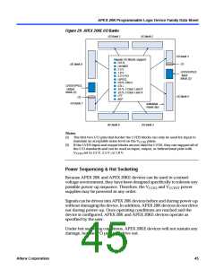
APEX 20K Programmable Logic Device Family Data Sheet
Clock Phase & Delay Adjustment
The APEX 20KE ClockShift feature allows the clock phase and delay to be
adjusted. The clock phase can be adjusted by 90° steps. The clock delay
can be adjusted to increase or decrease the clock delay by an arbitrary
amount, up to one clock period.
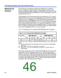
LVDS Support
Two PLLs are designed to support the LVDS interface. When using LVDS,
the I/ O clock runs at a slower rate than the data transfer rate. Thus, PLLs
are used to multiply the I/ O clock internally to capture the LVDS data. For
example, an I/ O clock may run at 105 MHz to support 840 megabits per
second (Mbps) LVDS data transfer. In this example, the PLL multiplies the
incoming clock by eight to support the high-speed data transfer. You can
use PLLs in EP20K400E and larger devices for high-speed LVDS
interfacing.
Lock Signals
The APEX 20KE ClockLock circuitry supports individual LOCKsignals.
The LOCKsignal drives high when the ClockLock circuit has locked onto
the input clock. The LOCKsignals are optional for each ClockLock circuit;
when not used, they are I/ O pins.
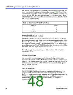
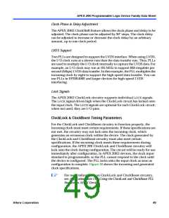
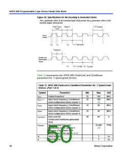
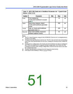
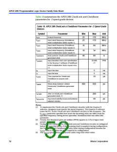
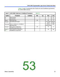
ClockLock & ClockBoost Timing Parameters
For the ClockLock and ClockBoost circuitry to function properly, the
incoming clock must meet certain requirements. If these specifications are
not met, the circuitry may not lock onto the incoming clock, which
generates an erroneous clock within the device. The clock generated by
the ClockLock and ClockBoost circuitry must also meet certain
specifications. If the incoming clock meets these requirements during
configuration, the APEX 20K ClockLock and ClockBoost circuitry will
lock onto the clock during configuration. The circuit will be ready for use
immediately after configuration. In APEX 20KE devices, the clock input
standard is programmable, so the PLL cannot respond to the clock until
the device is configured. The PLL locks onto the input clock as soon as
configuration is complete. Figure 30 shows the incoming and generated
clock specifications.
1
For more information on ClockLock and ClockBoost circuitry,
see Application Note 115: Using the ClockLock and ClockBoost PLL
Features in APEX Devices.
Altera Corporation
49

 ETC [ ETC ]