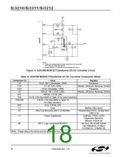
Si3210/Si3211/Si3212
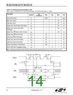
Table 10. Switching Characteristics—SPI
V
= V
= 3.13 to 5.25 V, T = 0 to 70°C for K-Grade, –40 to 85°C for B-Grade, C = 20 pF
DDA
DDA A L
Parameter
Test
Conditions
Symbol
Min
Typ
Max
Unit
Cycle Time SCLK
Rise Time, SCLK
Fall Time, SCLK
t
0.062
—
—
—
—
—
—
—
25
25
20
20
µsec
ns
c
t
r
t
—
ns
f
Delay Time, SCLK Fall to SDO Active
t
t
—
ns
d1
d2
Delay Time, SCLK Fall to SDO
Transition
—
ns
Delay Time, CS Rise to SDO Tri-state
Setup Time, CS to SCLK Fall
t
—
25
20
25
20
220
—
—
—
—
—
—
—
4
20
—
—
—
—
—
—
ns
ns
ns
ns
ns
ns
ns
d3
t
su1
Hold Time, CS to SCLK Rise
t
h1
Setup Time, SDI to SCLK Rise
Hold Time, SDI to SCLK Rise
Delay Time between Chip Selects
SDI to SDITHRU Propagation Delay
t
su2
t
h2
t
t
cs
cs
Note: All timing is referenced to the 50% level of the waveform. Input test levels are V = V
–0.4 V, V = 0.4 V
IH
DDD
IL
tthru
tr
tr
tc
SCLK
CS
tsu1
th1
tcs
tsu2
th2
SDI
td1
td3
td2
SDO
Figure 7. SPI Timing Diagram
14
Preliminary Rev. 1.11

 ETC [ ETC ]