Si3035
FSYNC
(mode 0)
FSYNC
(mode 1)
D15 D14 D13 D12 D11 D10 D9 D8 D7 D6 D5
D4 D3 D2 D1 D0
0
0
0
A
A
A
A
A
D
D
D
D
D
D
D
D
SDI
R/W
SDO
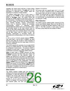
Figure 22. Secondary Communication Data Format—Write Cycle
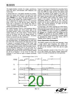
FUP1
FPLL1
FUP2
FPLL2
DIV
25
1
0
DIV N1
8 bits
DIV N2
4 bits
MCLK
DIV
5
PLL1
PLL2
1024·Fs
0
1
DIV M1
8 bits
DIV M2
4 bits
DIV
16
CGM
Bit
Figure 23. Clock Generation Subsystem
The architecture of the dual PLL scheme allows for fast Programming the Clock Generator
lock time on initial start-up, fast lock time when
As noted in Figure 23, the clock generator must output a
changing modem sample rates, high noise immunity,
and the ability to change modem sample rates with a
single register write. A large number of MCLK
frequencies between 1 MHz and 60 MHz are supported.
MCLK should be from a clean source, preferably
directly from a crystal with a constant frequency and no
dropped pulses.
"
clock equal to 1024 Fs, where Fs is the desired
"
sample rate. The 1024 Fs clock is determined through
programming of the following registers:
Register 7—N1 divider, 8 bits.
Register 8—M1 divider, 8 bits.
Register 9—N2/M2 dividers, 4 bits/4 bits.
Register 10—CGM, 1 bit.
In serial mode 2, the Si3021 operates as a slave device.
The clock generator is configured (by default) to set the
SCLK output equal to the MCLK input. The net effect is
the clock generator multiplies the MCLK input by 20. For
further details of slave mode operation, refer to "Multiple
Device Support" on page 25.
When using the Si3035 for modem applications, the
clock generator can be programmed to allow for a single
register write to change the modem sampling rate.
These standard sample rates are shown in Table 17.
The programming method is described below.
22
Rev. 1.2

 ETC [ ETC ]