Si3035
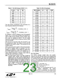
Table 17. N2, M2 Values (CGM = 0, 1)
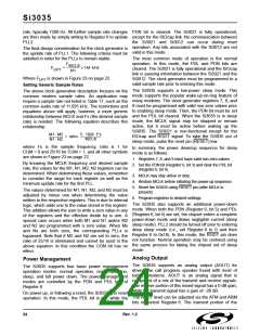
Table 18. MCLK Examples
Fs (Hz)
7200
8000
8229
8400
9000
9600
10286
N2
2
M2
2
MCLK (MHz)
1.8432
N1
1
M1
20
72
9
CGM
0
9
10
8
4.0000
5
1
7
4.0960
1
0
6
7
5.0688
11
5
80
48
6
0
4
5
6.0000
1
3
4
6.1440
1
0
7
10
8.1920
32
1
225
4
1
9.2160
0
The main design consideration is the generation of a
base frequency, defined as the following:
10.0000
10.3680
11.0592
12.288
25
9
144
32
10
3
1
0
F
M1
MCLK
= ---------------------------------- = 3 6. 8 64 M H z , C G M = 0
3
0
F
Base
N1
M1 16
1
0
F
MCLK
= --------------------------------------------- = 36.864MHz, CGM = 1
F
14.7456
16.0000
18.4320
24.5760
25.8048
33.8688
44.2368
46.0800
47.9232
48.0000
56.0000
60.0000
2
5
0
Base
N1 25
5
18
2
1
N1 (Register 7) and M1 (Register 8) are 8-bit unsigned
values. FMCLK is the clock provided to the MCLK pin.
Table 18 lists several standard crystal oscillator rates
that could be supplied to MCLK. This list simply
represents a sample of MCLK frequency choices. Many
more are possible.
1
0
32
7
75
10
160
125
4
1
0
147
96
5
0
After the first PLL has been setup, the second PLL can
be programmed easily. The values for N2 and M2
(Register 9) are shown in Table 17. N2 and M2 are 4-bit
unsigned values.
1
0
13
125
35
25
10
96
36
24
0
When programming the registers of the clock generator,
the order of register writes is important. For PLL1
updates, N1 (Register 7) must always be written first,
immediately followed by a write to M1 (Register 8). For
PLL2, the CGM bit must be set as desired prior to
writing N2/M2 (Register 9). Changes to the CGM bit
only take effect when N2/M2 are written.
0
1
1
PLL Lock Times
The Si3035 changes sample rates very quickly.
However, lock time will vary based on the programming
of the clock generator. The major factor contributing to
PLL lock time is the CGM bit. When the CGM bit is used
(set to 1), PLL2 will lock slower than when CGM is 0.
The following relationships describe the boundaries on
PLL locking time:
Note: The values shown in Table 17 and Table 18 satisfy the
equations above. However, when programming the
registers for N1, M1, N2, and M2, the value placed in
these registers must be one less than the value calcu-
lated from the equations. For example, for CGM = 0
with a MCLK of 48.0 MHz, the values placed in the N1
and M1 registers would be 0x7C and 0x5F, respec-
tively. If CGM = 1, a non-zero value must be pro-
grammed to Register 9 in order for the 16/25 ratio to
take effect.
PLL1 lock time < 1 ms (CGM = 0,1)
PLL2 lock time: 100 us to 1 ms (CGM = 0)
PLL2 lock time <1 ms (CGM = 1)
For modem designs, it is recommended that PLL1 be
programmed
during
initialization.
No
further
programming of PLL1 is necessary. The CGM bit and
PLL2 can be programmed for the desired initial sample
Rev. 1.2
23

 ETC [ ETC ]