Si3035
rate, typically 7200 Hz. All further sample rate changes PDN bit is cleared. The Si3021 is fully operational,
are then made by simply writing to Register 9 to update except for the ISOcap link. No communication between
PLL2.
the Si3021 and Si3012 can occur during reset
operation. Any bits associated with the Si3012 are not
valid in this mode.
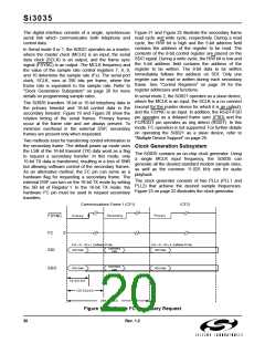
The final design consideration for the clock generator is
the update rate of PLL1. The following criteria must be
satisfied in order for the PLLs to remain stable:
The most common mode of operation is the normal
operation. In this mode, the PDL and PDN bits are
cleared. The Si3021 is fully operational and the ISOcap
link is passing information between the Si3021 and the
Si3012. The clock generator must be programmed to a
valid sample rate prior to entering this mode.
F
MCLK
N1
F
= --------------------- ≥ 144 kHz
UP1
Where FUP1 is shown in Figure 23 on page 22.
Setting Generic Sample Rates
The Si3035 supports a low-power sleep mode. This
mode supports the popular wake-up-on-ring feature of
many modems. The clock generator registers 7, 8, and
9 must be programmed with valid non-zero values prior
to enabling sleep mode. Then, the PDN bit must be set
and the PDL bit cleared. When the Si3035 is in sleep
mode, the MCLK signal may be stopped or remain
active, but it must be active before waking up the
Si3035. The Si3021 is non-functional except for the
ISOcap and RGDT signal. To take the Si3035 out of
sleep mode, pulse the reset pin (RESET) low.
The above clock generation description focuses on the
common modem sample rates. An application may
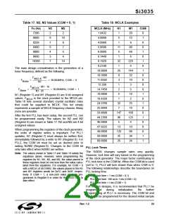
require a sample rate not listed in Table 17, such as the
common audio rate of 11.025 kHz. The restrictions and
equations above still apply; however, a more generic
relationship between MCLK and Fs (the desired sample
rate) is needed. The following equation describes this
relationship:
5 1024 Fs
--------------------------------
M1 M2
N1 N2
--------------------- = r a t i o
MCLK
where Fs is the sample frequency, ratio is 1 for
CGM = 0 and 25/16 for CGM = 1, and all other symbols
are shown in Figure 23 on page 22.
In summary, the power down/up sequence for sleep
mode is as follows:
1. Registers 7, 8, and 9 must have valid non-zero values.
By knowing the MCLK frequency and desired sample
rate, the values for the M1, N1, M2, N2 registers can be
determined. When determining these values, remember
to consider the range for each register as well as the
minimum update rate for the first PLL.
2. Set the PDN bit (Register 6, bit 3) and clear the PDL bit
(Register 6, bit 4).
3. MCLK may stay active or stop.
4. Restore MCLK before initiating the power-up sequence.
5. Reset the Si3035 using RESET pin (after MCLK is
present).
The values determined for M1, N1, M2, and N2 must be
adjusted by minus one when determining the value
written to the respective registers. This is due to internal
logic, which adds one to the value stored in the register.
This addition allows the user to write a zero value in any
of the registers and the effective divide by is one. A
special case occurs when both M1 and N1 and/or M2
and N2 are programmed with a zero value. When Mx
and Nx are both zero, the corresponding PLLx is
bypassed. Note that if M2 and N2 are set to zero, the
ratio of 25/16 is eliminated and cannot be used in the
above equation. In this condition the CGM bit has no
effect.
6. Program registers to desired settings.
The Si3035 also supports an additional power-down
mode. When both the PDN (Register 6, bit 3) and PDL
(Register 6, bit 4) are set, the chipset enters a complete
power-down mode and draws negligible current (deep
sleep mode). PLL2 should be turned off prior to entering
deep sleep mode (i.e., set Register 9 to 0 and then
Register 6 to 0x18). In this mode, the RGDT pin does
not function. Normal operation may be restored using
the same process for taking the chipset out of sleep
mode.
Analog Output
Power Management
The Si3035 supports an analog output (AOUT) for
driving the call progress speaker found with most of
today’s modems. AOUT is an analog signal that is
comprised of a mix of the transmit and receive signals.
The receive portion of this mixed signal has a 0 dB gain,
while the transmit signal has a gain of –20 dB.
The Si3035 supports four basic power management
operation modes: normal operation, reset operation,
sleep, and full power down. The power management
modes are controlled by the PDN and PDL bits of
Register 6.
On power up, or following a reset, the Si3035 is in reset
operation. In this mode, the PDL bit is set, while the
The AOUT level can be adjusted via the ATM and ARM
bits in control Register 6. The transmit portion of the
24
Rev. 1.2

 ETC [ ETC ]