Si3035
procedure:
Functional Description
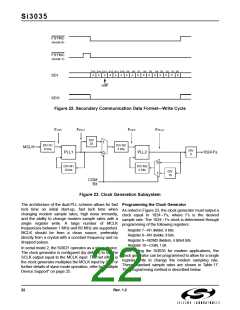
1. Program the PLLs with registers 7 to 9 (N1[7:0], M1[7:0],
N2[3:0] and M2[3:0]) to the appropriate divider ratios for
the supplied MCLK frequency and desired sample rate, as
defined in "Clock Generation Subsystem" on page 20.
The Si3035 is an integrated chipset that provides a
low-cost, isolated, silicon-based interface to the
telephone line. The Si3035 saves cost and board area
by eliminating the need for a modem AFE or serial
codec. It also eliminates the need for an isolation
transformer, relays, opto-isolators, and a 2- to 4-wire
hybrid. The Si3035 solution requires only a few
low-cost, discrete components to achieve full
compliance with FCC Part 68 and JATE out-of-band
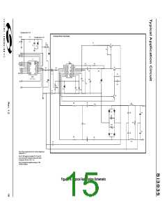
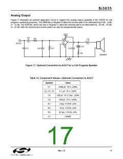
noise requirements. See Figure 16 on page 15 for a
typical application circuit. See the pin-compatible
Si3034 or Si3044 data sheets for designs requiring
global support.
2. Wait until the PLLs are locked. This time is between
100 µS and 1 ms.
3. Write an 0x80 into Register 6. This enables the charge
pump for the VA pin, powers up the line-side chip (Si3012),
and enables the AOUT for call progress monitoring.
After this procedure is complete, the Si3035 is ready for
ring detection and off-hook.
Isolation Barrier
The Si3035 achieves an isolation barrier through a
The Si3035 North America/Japan DAA offers a number low-cost, high-voltage capacitor in conjunction with
of new features not supported by the Si3032 device. Silicon Laboratories’ proprietary ISOcap signal
These include operation from a single 3.3 V power processing techniques. These techniques eliminate any
supply, JATE (Japan) filter option, finer resolution for signal degradation due to capacitor mismatches,
both transmit and receive levels on AOUT (call progress common mode interference, or noise coupling. As
output), daisy-chaining for up to eight devices, and an shown in Figure 16 on page 15, the C1, C2, and C4
optional IIR filter. Table 15 summarizes the new Si3035 capacitors isolate the Si3021 (DSP-side) from the
features.
Si3012 (line-side). All transmit, receive, control, and
caller ID data are communicated through this barrier.
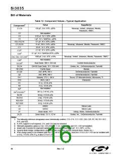
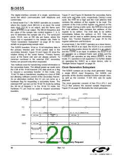
Table 15. New Si3035 Features
The ISOcap inter-chip communication is disabled by
default. To enable it, the PDL bit in Register 6 must be
cleared. No communication between the Si3021 and
Si3012 can occur until this bit is cleared. The clock
generator must be programmed to an acceptable
sample rate prior to clearing the PDL bit.
Category
Daisy-Chaining
Si3032
—
Si3035
Up to 8 Devices
Yes
Optional IIR Filter
Receive Gain
—
Off-Hook
0, 6 dB
0, –3 dB
0, 3, 6, 9, 12 dB
The communication system generates an off-hook
command by applying logic 0 to the OFHK pin or writing
a logic 1 to bit 0 of control Register 5. The OFHK pin
must be enabled by setting bit 1 (OHE) of Register 5.
With OFHK at logic 0, the system is in an off-hook state.
This state is used to seize the line for incoming/outgoing
calls and can also be used for pulse dialing. With OFHK
at logic 1, negligible DC current flows through the
hookswitch. When a logic 0 is applied to the OFHK pin,
the hookswitch transistor pair, Q1 and Q2, turn on. The
net effect of the off-hook signal is the application of a
termination impedance across TIP and RING and the
flow of DC loop current. The termination impedance has
both an AC and a DC component.
Transmit Attenuation
0, –3, –6 –9,
–12 dB
VA
VD
5 V
3.3 V* or 5 V
3.3 V or 5 V
3.3 V or 5 V
JATE Support
—
Yes
AOUT Levels (dB)
0, mute
0, –6, –12, mute
*Note: The VA supply is internally generated by an on-chip
charge pump.
Initialization
The AC termination impedance is a 604-Ω resistor,
which is connected to the TX pin. The DC termination is
a 51-Ω resistor, which is connected to the DCT pin.
When the Si3035 is initially powered up, the RESET pin
should be asserted. When the RESET pin is
deasserted, the registers will have default values. This
reset condition guarantees the line-side chip (Si3012) is
powered down with no possibility of loading the line (i.e.,
off-hook). The following is an example initialization
When executing an off-hook sequence, the Si3035
requires 1548/Fs seconds to complete the off-hook and
provide phone line data on the serial link. This includes
the 12/Fs filter group delay. If necessary, for the shortest
18
Rev. 1.2

 ETC [ ETC ]