Si3035
delay, a higher Fs may be established prior to executing
Improved JATE Support
the off-hook, such as an Fs of 10.286 kHz. The delay
allows line transients to settle prior to normal use.
The HYBD pin connects to a node on the internal hybrid
cancellation circuit providing a pin for a balancing
capacitor, C12. C23 adds the necessary transmit
out-of-band filtering required to meet JATE out-of-band
noise specifications. The addition of C23 alters the
transmit path frequency response which must be
balanced with capacitor C12 to obtain maximum hybrid
cancellation.
Ring Detect
The ring signal enters the Si3035 through low value
capacitors connected to TIP and RING. RGDT is a
clipped, half-wave rectified version of the ringing
waveform. See Figure 18 for a timing diagram of the
RGDT pin.
Products using the Si3035 which have been submitted
for JATE approval should document a waiver for the
JATE DC Termination specification. This specification is
met in the Si3034 global DAA device.
The integrated ring detect of the Si3035 allows the
device to present the ring signal to the DSP, through the
serial port, with no additional signaling required. The
signal sent to the DSP is a clipped version of the original
ring signal. In addition, the Si3035 passes through the
caller ID data unaltered.
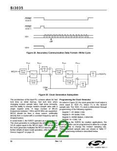
Digital Interface
The Si3035 has two serial interface modes that support
The system can also detect an occurring ring by the most standard modem DSPs. The M0 and M1 mode
status of the RDT bit of Register 5. This bit is a pins select the interface mode. The key difference
read-only bit that is set when the line-side device between these two serial modes is the operation of the
detects a ring signal at RNG1 and RNG2. The RDT bit FSYNC signal. Table 16 summarizes the serial mode
clears when the system either goes off-hook or 4.5 to 9 definitions.
seconds after the last ring is detected.
Table 16. Serial Modes
If caller ID is supported in the system, the designer can
enable the Si3035 to pass this information to the SDO
Mode M1 M0
Description
output. Following the completion of the first ring, the
system should set the ONHM bit (Register 5, bit 3). This
bit must be cleared at the conclusion of the receipt of
the caller ID data and prior to the next ring burst.
0
1
2
3
0 0 FSYNC frames data
0 1 FSYNC pulse starts data frame
1 0 Slave mode
The Si3021 can support a wake-up-on-ring function
using the RGDT signal. Refer to "Power Management"
on page 24 for more details
1 1 Reserved
.
First Ring
0.2–3.0 seconds
> 0.2 Sec.
0.5–1.5 Sec.
RNG1/
RNG2
DATA
RGDT
SDO
DIGITIZED LINE SIGNAL
Figure 18. Ring Detect Timing
Rev. 1.2
19

 ETC [ ETC ]