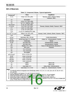
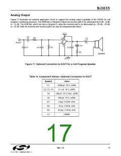
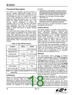
Si3035
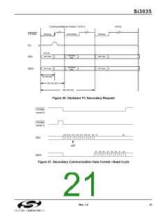
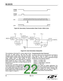
The digital interface consists of a single, synchronous Figure 21 and Figure 22 illustrate the secondary frame
serial link which communicates both telephony and read cycle and write cycle, respectively. During a read
control data.
cycle, the R/W bit is high and the 5-bit address field
contains the address of the register to be read. The
contents of the 8-bit control register are placed on the
SDO signal. During a write cycle, the R/W bit is low and
the 5-bit address field contains the address of the
register to be written. The 8-bit data to be written
immediately follows the address on SDI. Only one
register can be read or written during each secondary
frame. See "Control Registers" on page 34 for the
register addresses and functions.
In Serial mode 0 or 1, the Si3021 operates as a master,
where the master clock (MCLK) is an input, the serial
data clock (SCLK) is an output, and the frame sync
signal (FSYNC) is an output. The MCLK frequency and
the value of the sample rate control registers 7, 8, 9,
and 10 determine the sample rate (Fs). The serial port
clock, SCLK, runs at 256 bits per frame, where the
frame rate is equivalent to the sample rate. Refer to
"Clock Generation Subsystem" on page 20 for more
details on programming sample rates.
In serial mode 2, the Si3021 operates as a slave device,
where the MCLK is an input, the SCLK is a no connect
(except for the master device for which it is an output),
and the FSYNC is an input. In addition, the RGDT/FSD
pin operates as a delayed frame sync (FSD) and the
FC/RGDT pin operates as ring detect (RGDT). In this
mode, FC operation is not supported. For further details
on operating the Si3021 as a slave device, refer to
"Multiple Device Support" on page 25.
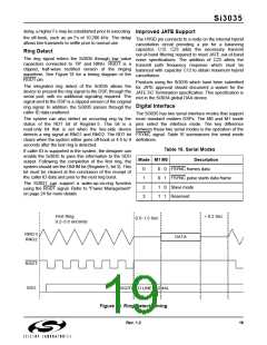
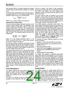
The Si3035 transfers 16-bit or 15-bit telephony data in
the primary timeslot and 16-bit control data in the
secondary timeslot. Figure 19 and Figure 20 show the
relative timing of the serial frames. Primary frames
occur at the frame rate and are always present. To
minimize overhead in the external DSP, secondary
frames are present only when requested.
Two methods exist for transferring control information in
the secondary frame. The default power-up mode uses
the LSB of the 16-bit transmit (TX) data word as a flag
to request a secondary transfer. In this mode, only
15-bit TX data is transferred, resulting in a loss of SNR
but allowing software control of the secondary frames.
As an alternative method, the FC pin can serve as a
hardware flag for requesting a secondary frame. The
external DSP can turn on the 16-bit TX mode by setting
the SB bit of Register 1. In the 16-bit TX mode, the
hardware FC pin must be used to request secondary
transfers.
Clock Generation Subsystem
The Si3035 contains an on-chip clock generator. Using
a single MCLK input frequency, the Si3035 can
generate all the desired standard modem sample rates,
as well as the common 11.025 kHz rate for audio
playback.
The clock generator consists of two PLLs (PLL1 and
PLL2) that achieve the desired sample frequencies.
Figure 23 on page 22 illustrates the clock generator.
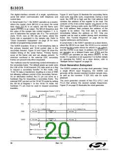
Communications Frame 1 (CF1)
(CF2)
Secondary
Prim ary
Prim ary
FSYNC
FC
0
D15 – D1 D0 = 1 (Software FC Bit)
D15 – D1 D0 = 0 (Software FC Bit)
XMT Data
Secondary
XMT Data
SDI
Data
Secondary
Data
RCV Data
RCV Data
SDO
16 SCLKS
128 SCLKS
256 SCLKS
Figure 19. Software FC Secondary Request
20
Rev. 1.2

 ETC [ ETC ]