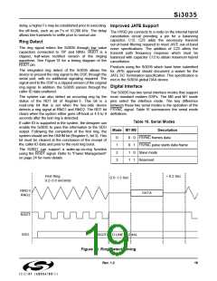
Decoupling cap for U1 VD
No Ground Plane In DAA Section
VCC
R3
10
Decoupling cap for U1 VA
C10
R1
D3
Q1
BAV99
C3
Z4
R5
M0
RGDTb
OFHKb
U1
1
2
3
4
5
6
7
8
16
U2
Si3012
MCLK
FSYNCb
SCLK
MCLK
FSYNC
SCLK
VD
SDO
SDI
OFHK
15
R4
R21
RGDT
14
1
2
3
4
5
6
7
8
16
15
14
13
12
11
10
9
M0
13
TSTA
TSTB
IGND
C1B
TX
NC2
RX
REXT
DCT
Q2
VA
12
R27
R28
SDO
SDI
FC
GND
11
C1A
10
C5
R18
FC
RESET
M1
9
RNG1
RESETb
AOUT
RNG2 HYBD
C1
R6
QB
QE
VREG2
VREG
Si3021
SOIC Pinout
C23
+
C12
AOUT
M1
C30
Z1
R2
C20
D4
BAV99
Z5
C6
C16
C2
Q3
C8
R23
FB2
R10
RING
D2
C9
C25
C32
RV1
C11
RV2
D1
C31
C24
R22
C7
R9
TIP
FB1
C4
Note 1: R3 is not required when Vcc=3.3 V and the charge pump is
enabled (CPE = 1).
Note 2: If JATE support is not required, R21, C12 and C23
may be removed (R21 is effectively 0 ohms) and R4 should
be changed to a 604 ohm, 1/4 W, +- 1%.
Note 3: See Appendix for applications requiring UL 1950
3rd Edition compliance.
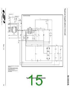
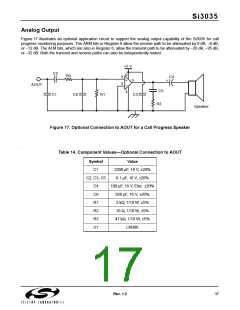
Figure 16. Typical Application Schematic

 ETC [ ETC ]