PCT2303N DATA SHEET
FUNCTIONAL DESCRIPTION
!!
Slot 5: Modem Line 1 Codec
The first bit (MSB) sampled by the PCT303A indicates
whether the current control transaction is a read or a
write operation. The following seven bit positions
communicate the targeted control register address. The
trailing 12 bit positions within the slot are reserved and
must be padded with 0s by the AC’97 controller.
Modem output frame slot 5 contains the MSB justified
modem DAC input data for phone line #1.
The PCT2303N’s modem DAC input resolution is 16
bits.
Slot 10: Modem Line 2 DAC
Slot 2: Command Data Port
Line 2 is assigned to slot 10. The leading 16 bits of each
slot must contain valid sample data (MSB bit 19, LSB 4).
The command data port delivers 16-bit control register
write data in the event that the current command port
operation is a write cycle as indicated by Slot 1, bit 19.
Slot 12: Modem GPIO Control
Slot 12 contains latency critical signals for the PCT303L
and the GPIO of the PCT303A. See Table 4.
Command Data Port bit assignments:
• Bits 19:4—Control register write data (padded with 0s if
the current operation is a read)
Slots 3, 4, 6–9, 11: Not Used
The PCT2303N always pads audio output frame slots 3,
4, 6–9, and 11 with 0s.
• Bits 3:0—Reserved (padded with 0s)
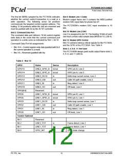
Table 4 Slot 12
GPIO
Name
Sense
in/out
in/out
in
Description
GPIO15
GPIO14
GPIO13
GPIO12
GPIO11
GPIO10
GPIO[9:6]
GPIO5
GPIO4
GPIO3
GPIO2
GPIO1
GPIO0
Vendor Optional
Bit 3
LINE2_GPIO_B
LINE2_GPIO_A
LINE2_DLCS
LINE2_CID
LINE2_RI
GPIO pin B, Line 2
GPIO pin A, Line 2
Delta loop current sense, Line 2
Caller ID path enable, Line 2
Ring detect, Line 2
out
in
LINE2_OH
out
Off hook, Line 2
Reserved
LINE1_GPIO_B
LINE1_GPIO_A
LINE1_DLCS
LINE1_CID
LINE1_RI
in/out
in/out
in
GPIO pin B, Line 1
GPIO pin A, Line 1
Delta loop current sense, Line 1
Caller ID path enable, Line 1
Ring detect, Line 1
out
in
LINE1_OH
out
Off hook, Line 1
Reserved
Bit 2
LINE2_FDT
LINE1_FDT
GPIO_INT
in
in
in
Frame detect, Line 2
Frame detect, Line 1
GPIO state change
Bit 1
Bit 0
PC-TEL, Inc.
12
2303N0DOCDAT10A-0899

 ETC [ ETC ]