Functional Description
• Below 1 MB option that supports compatible SMI handlers.
• Above 1 MB option that allows new SMI handlers to execute with write-back cacheable
SMRAM.
• Optional larger write-back cacheable T_SEG area from 128KB to 1MB in size above 1 MB
that is reserved from the highest area in system DRAM memory. The above 1 MB solutions
require changes to compatible SMRAM handlers code to properly execute above 1 MB.
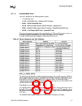
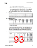
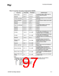
Table 4-2 summarizes the operation of SMRAM space cycles targeting the SMI space addresses.
Table 4-2. SMRAM Decoding
Name of Range
Transaction Address
A0000–BFFFFh
DRAM Address
A0000–BFFFFh
compatible (Range A)
HI-SMRAM (RANGE H)
TSEG (RANGE T)
256M + A0000h to 256M + FFFFFh
A0000–FFFFFh
256M + TOM to 256M + TOM - TSEG_SIZE
TOM to TOM - TSEG_SIZE
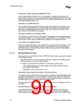
Table 4-3. SMRAM Range Decode
Global SMRAM
H_SMRAME
TSEG_EN
A Range
H Range
T Range
0
1
1
1
1
x
0
0
1
1
x
0
1
0
1
Disable
Enable
Disable
Disable
Disable
Enable
Enable
Disable
Disable
Enable
Disable
Enable
Enable
Disabled
Disabled
NOTE:
1. 1 = Enabled and 0 = Disabled
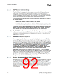
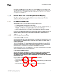
Table 4-4 defines the control of the decode for all code fetches and data fetches to SMRAM ranges
(as defined by Table 4-3). The G_SMRAM bit provides a global disable for all SMRAM memory.
The D_OPEN bit allows software to write to the SMRAM ranges without being in SMM. BIOS
software can use this bit to initialize SMM code at Power up. The D_LCK bit limits the SMRAM
range access to only SMM mode accesses. The D_CLS bit causes SMM data accesses to be
forwarded to PCI. The SMM software can use this bit to write to video memory while running code
out of DRAM.
Table 4-4. SMRAM Decode Control
SMM Code
Fetch
SMM Data
Fetch
G_SMRAME
D_LCK
D_CLS
D_OPEN
SMM Mode
0
1
1
1
1
1
1
1
1
x
0
0
0
0
0
1
1
1
x
x
0
0
1
1
x
0
1
x
0
0
1
0
1
x
x
x
x
0
1
x
1
x
0
1
1
Disable
Disable
Enable
Enable
Enable
Invalid
Disable
Disable
Enable
Enable
Disable
Invalid
Disable
Enable
Enable
Disable
Enable
Disable
NOTE:
1. 1 = Enabled and 0 = Disabled
82443BX Host Bridge Datasheet
4-7

 ETC [ ETC ]