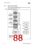
Functional Description
4.1.1.3
AGP Memory Address Range
The 82443BX can be programmed to direct memory accesses to the AGP bus interface when
addresses are within either of two ranges specified via registers in 82443BX Device #1
configuration space. The first range is controlled via the Memory Base Register (MBASE) and
Memory Limit Register (MLIMIT) registers. The second range is controlled via the Prefetchable
Memory Base (PMBASE) and Prefetchable Memory Limit (PMLIMIT) registers
The 82443BX positively decodes memory accesses to AGP memory address space as defined by
the following equations:
≤
≤
Memory_Base_Address Address Memory_Limit_Address
≤
≤
Prefetchable_Memory_Base_Address Address Prefetchable_Memory_Limit_Address
The effective size of the range is programmed by the plug-and-play configuration software and it
depends on the size of memory claimed by the AGP compliant device. Normally, these ranges
reside above the Top-of-Main-DRAM and below High BIOS and APIC address ranges.
Note: The 82443BX Device #1 memory range registers described above are used to allocate memory
address space for any devices on AGP that require such a window. These devices include the AGP
compliant device, and multifunctional AGP compliant devices where one or more functions are
implemented as PCI devices.
4.1.1.4
AGP DRAM Graphics Aperture
Memory-mapped, graphics data structures can reside in a Graphics Aperture to main DRAM
memory. This aperture is an address range defined by the APBASE configuration register of the
82443BX Host Bridge. The APBASE register follows the normal base address register template as
defined by the PCI 2.1 specification. The size of the range claimed by the APBASE is programmed
via “back-end” register APSIZE (programmed by the chip-set specific BIOS before plug-and-play
session is performed). APSIZE allows selection of the aperture size of 4 MB, 8 MB,16 MB,
32 MB, 64 MB, 128 MB and 256 MB. By programming APSIZE to a specific size, the
corresponding lower bits of APBASE are forced to “0” (behave as hardwired). Default value of
APSIZE forces aperture size of 256 MB. Aperture address range is naturally aligned.
Although this aperture appears to be established in PCI memory space, in fact the 82443BX
forwards accesses within the aperture range to the main DRAM subsystem. The originally issued
addresses are translated (within 82443BX’s DRAM controller subsystem) via a translation table
maintained in main memory. Translation table entries may be partially cached in a Graphics
Translation Look-aside Buffer (GTLB) implemented within the 82443BX’s DRAM subsystem.
The aperture range will not be cacheable in the processor caches.
4.1.1.5
System Management Mode (SMM) Memory Range
82443BX supports the use of main memory as System Management RAM (SMRAM) enabling the
use of System Management Mode. The 82443BX supports two SMRAM options: Compatible
SMRAM (C_SMRAM) and Extended SMRAM (E_SMRAM). System Management RAM
(SMRAM) space provides a memory area that is available for the SMI handler's and code and data
storage. This memory resource is normally hidden from the system OS so that the processor has
immediate access to this memory space upon entry to SMM. The 82443BX provides three
SMRAM options:
4-6
82443BX Host Bridge Datasheet

 ETC [ ETC ]