AN-35
RCABLE
with stable dielectrics (NPO or COG, for example) are higher
cost.Thevalueoflowcostceramiccapacitorsvariessignificantly
withvoltageandtemperature(Z5Udielectric, forexample)and
should not be used since they may cause output oscillation.
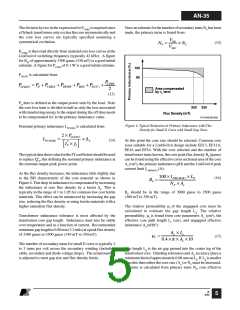
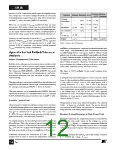
RLOAD
RINT_RES
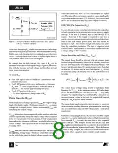
RCABLE = 0.23 Ω
RINT_RES = 0.5 Ω
RLOAD= 11 Ω
CONTROL Pin Capacitor (CCP)
2 x 1N4001
10,000 µF
CCP sets the auto-restart period and also the time the output has
to reach regulation before entering auto-restart at power supply
start-up. If the load is a battery, then a value of 0.22 µF is
typical. However, if the supply is required to start into a
resistiveloadorconstantcurrentload(suchasabenchelectronic
load) at the peak output power point, then this should be
increased to 1 µF. This ensures enough time during start-up to
bring the output into regulation. The type of capacitor is not
critical. Either a small ceramic or electrolytic may be used with
a voltage rating of 10 V or more.
PI-2975-072402
Figure 7. Example of Battery Model Load (Values for a Typical
3 W, 5.5 V Battery Charger).
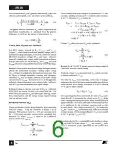
Atno-load,increasingRLF slightlyincreasestheno-loadvoltage
sincetheprimaryleakageinductanceisfilteredmoreeffectively,
butthesamepeakchargingduetosecondaryleakageinductance
occurs. Although the no-load voltage is slightly higher, there is
only a minor effect on no-load consumption.
Output Rectifier and Filter (DOUT, COUT
)
The output diode should be selected with an adequate peak
inverse voltage (PIV) rating. Either PN or Schottky diodes can
be used. Schottky diodes offer higher efficiency at higher cost
but provide the most linear CC output characteristic. Both fast
or ultra fast PN diodes may be used, but ultra fast (trr~50 ns)
are preferred giving CC linearity close to the performance of a
Schottky.
In a design that has high leakage, the value of RFB can be
increasedtoraisetheoveralloutputvoltage(Figure6). However,
this will also increase no-load voltage and therefore no-load
input power consumption.
To iterate RLF:
NS
NP
(26)
• Start with typical value of 100 Ω and a transformer with
nominal inductance.
PIV DOUT ≥ V
×
+ V ×1.5
(
)
DC(MAX)
O
• Verify CC portion of the curve and increase or decrease
RLF until CC curve is approximately vertical (current at
start of CC and end are approximately the same)
• Verify CV portion of the curve.
The output diode voltage rating should be calculated from
Equation 26. VDC(MAX) is the maximum primary DC rail voltage
(375 V for universal or 230 VAC and 187 V for 115 VAC only
designs). TheoutputvoltageVO ismultipliedby1.5toallowfor
increased output voltage at no-load. An output diode current
rating of 2 x IO is a good initial estimate.
- For minor adjustment, change value of RFB.
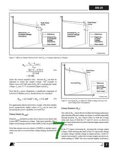
Clamp Capacitor (CCLAMP
)
WithsmallvaluesofclampcapacitorCCLAMP, theoutputvoltage
tendstobeslightlyhigher. WithlargervaluesforCCLAMP,output
voltage will be slightly lower. Further increases in CCLAMP will
not change the output voltage.
The output diode may be placed in either the upper or lower leg
of the secondary winding. However, placement in the lower leg
may provide lower conducted EMI with a suitably constructed
transformer.
CCLAMP isthereforechosenempiricallyasthesmallestvaluethat
doesnotsignificantlychangetheoutputvoltagewhencompared
to the next larger value. For most designs, 100 nF is typical and
standard device tolerances will have a negligible effect on the
output voltage. This capacitor should be rated above the VOR,
typically 100 V.
For battery charger applications, the size and cost of the output
capacitorCOUT canbesignificantlyreduced. Highripplecurrent
flows through COUT for only the short time a fully depleted
battery charges. The designer should take into account that
COUT ripple current rating can be exceeded for short periods of
time without reducing lifetime significantly. When the battery
is close to fully charged, the LinkSwitch circuit transitions to
CV mode, where capacitor ripple current is much smaller.
CCLAMP must have a stable value over temperature and also over
the operating voltage range. Metalized plastic film capacitors
are the best choice, since the higher voltage ceramic capacitors
B
4/03
8

 ETC [ ETC ]