AN-35
Other gapping techniques allow tighter tolerances, but may not
be universally supported, so again, this should be verified with
the preferred magnetics vendor. Film gapping, where thin
materialspacesallthreelegsofthecore,allowsbettermechanical
tolerance and improves overall primary inductance tolerance to
7% with a 0.05 mm gap. Since a gap now appears on the outer
legs of the core, flux spraying may result, causing pick up in the
input filter components and resulting in poorer than expected
conducted EMI. This can be prevented, if necessary, by adding
a single shorted turn of copper foil around the outside of the
transformer core also known as a “belly band.”
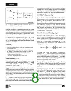
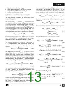
Reducing No-load Voltage with a Pre-load
At very light loads (< ~5 mA), the output voltage rises due to
secondary peak charging. This can be significantly reduced by
the addition of a small pre-load resistor. Figure 10 shows the
effect of a 1 mA and 2 mA pre-load on a 9 V output design,
reducingtheno-loadvoltageby1.3V.Thislevelofpre-loadhas
minimal effect on no-load consumption (~10 mW to 20 mW).
Minimizing No-Load Consumption
The major factors for no-load or standby consumption are PBIAS
and the capacitive switching loss PC(LOSS) (Equations 9 and 28). If
no-load consumption is too high, then the transformer may be
redesigned with a lower VOR.
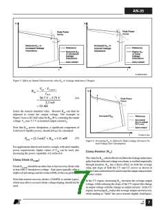
Core gaps should be uniform. Uneven core gapping (see
Figure 8), especially with small gap sizes, may cause variation
in the primary inductance with flux density (partial saturation)
and make the constant current region nonlinear. To verify
uniform gapping, it is recommended that the primary switching
current waveshape be examined while feeding the supply from
a DC source. The slope is defined as di/dt = V/L and should
remain constant throughout the MOSFET on time. Any change
in slope of the current ramp is an indication of uneven gapping.
Total parasitic capacitance of device and transformer, typically
25 pF to 30 pF, causes a switching loss that increases with input
voltageandhasasignificanteffectonstandbyorno-loadoutput
power consumption.
CTOT × VM2AX × fS
(28)
P
=
C(LOSS)
Verifying Discontinuous Mode Operation
2
To verify a design will remain discontinuous conduction mode
under worst case condition use Equation 27:
VMAX is typically 340 V for universal or 230 VAC applications
and fS is 30 kHz at light or no load. Parasitic capacitance loss
PC(LOSS) is typically 40 mW to 100 mW. This loss is not included
in the LP calculation as this power is not processed through the
core.
2 × IO(MAX) × fS(MAX) × LP(MAX)
NP
<
(27)
D × (1− D) × VDC(MIN)
NS
To minimize transformer capacitance, double coated magnet
wire should be used for the primary winding. The technique of
vacuum impregnation should not be used since the varnish acts
as adielectric, increasingwindingcapacitance. Dipvarnishing
does not cause this problem.
whereIO(MAX) istheoutputcurrent(A)atmaximumCCtolerance
(typically IO(NOM) + 20%), fS(MAX) is the maximum LinkSwitch
switchingfrequency(Hz), LP(MAX) istheprimaryinductance(H)
at maximum tolerance, D is duty cycle at minimum input
voltage (typically 0.3 at 85 VAC or 0.13 at 195 VAC) and
VDC(MIN) the minimum DC voltage at lowest input line voltage
(typically 100 VDC for 85 VAC and 230 VDC for 195 VAC).
An RC snubber placed across the output diode also increases
no-load consumption. If necessary, minimize the value of the
Effect of Output Cable
15
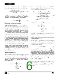
Factors such as leakage inductance, the value for RLF, RFB and
CCLAMPhavebeencovered. However,thereareotherparameters
that should be considered when designing with LinkSwitch.
No pre-load
1 mA pre-load
2 mA pre-load
12
9
Ifthegaugeofwireselectedfortheoutputcableisreduced,then
the voltage drop across the cable resistance will increase. As
seen at the load, this appears as poorer CV operation and lower
efficiency, but with the CV/CC transition at the same output
current(seeFigure9). Ensurethatthevoltagedroporresistance
of the output cable is acceptable.
0
4
8
12
Output Current (mA)
PI-3227-082202
Figure 10. A Small Pre-load can Significantly Reduce No-load
Voltage.
B
4/03
10

 ETC [ ETC ]