AN-35
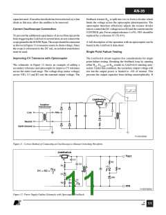
desired, a 0.5 W Zener can be added across the output to clamp
this voltage rise. The Zener voltage should be set above the
normal maximum output voltage at no-load. Short circuiting or
opening CCP safely prevents LinkSwitch operation.
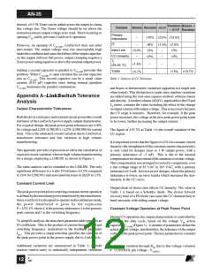
Random
+ ∆I/∆V
Biases +
Random
Variable Biases Random ∆I/∆V
Primary
–
10%
2.5% 12.5%
Inductance
I2f
–
3.2%
–
6%
3%
2%
1.5%
7.5%
3%
However, on opening of CCLAMP, LinkSwitch does not enter
auto-restart. The output voltage may rise unacceptably high
underthisconditionandcausethefailureoftheoutputcapacitor.
As the supply delivers full power, output clamping requires a
Zenerpowerratingequaltoorabovethenominaloutputpower.
Input Line
–
–
CC Linearity
Tj
(25-65 C)
2%
–
–
–
1.5%
4.7%
°
Adding a second capacitor in parallel to CCLAMP prevents this
problem. When CCLAMP is open circuited the second capacitor
acts as CCLAMP. This second capacitor can be a small value
ceramic (0.01 µF) capacitor since during normal operation
CCLAMP dominates the parallel combination.
Totals
15%
19.7%
Table 1. Sources of CC Tolerance.
and biases or deterministic variations (apparent in a single unit
when tested). This distinction is made since random variations
are added using the root-sum-squares method, whereas biases
adddirectly. Afurthercolumn(∆I/∆V),applicabletotheI2fand
LP terms, contains the value including the effect of the change
inoutputcurrentwithoutputvoltage. Thisisnecessarybecause
the CV slope is nonzero. Therefore, for example, if the peak
power increases, the voltage at the new peak power point tends
to be lower, further increasing the output current.
Appendix A–LinkSwitch Tolerance
Analysis
Output Characteristic Tolerances
Boththedevicetoleranceandexternalcircuitgoverntheoverall
tolerance of the LinkSwitch power supply output characteristic.
For a typical design, the peak power point tolerances are 10%
for voltage and 20% (LNK501) / 25% (LNK500) for current
limit. This is the estimated overall variation due to LinkSwitch,
transformer tolerance and line variation in high volume
manufacturing.
The figure of 19.7% in Table 1 is the overall variation of the
CC region.
Itisimportanttonotethatthefigureof 2%forconstantcurrent
linearity (the straightness of the constant current characteristic)
is only valid for designs close to 3 W output power, with a
primary inductance of ~3 mH. This is due to the internal
compensationfordraincurrentdi/dtvariationsoverlinevoltage.
This compensation was arranged to correctly compensate, over
a line voltage range of 85 VAC to 265 VAC, with a primary
inductanceof3mH. Inlowerpowerdesigns,wheretheprimary
inductance is lower, an error results which increases the non-
linearity in the CC curve.
This appendix provides expressions to allow the calculation of
expected circuit variation when in high volume manufacturing
for a design employing a LNK501 as shown in Figure 3.
The same analysis can be extended to the LNK500. The only
significant difference is a wider I2f tolerance ( 12% compared
to 6% for LNK501) and associated increase in ∆I/∆V to 3%.
Constant Current Limit
Output diode of choice also effects CC linearity. The value in
Table 1 is based on a Schottky diode. The slower forward
recovery time of a PN diode can cause the CC characteristic to
bend outwards with falling output voltage.
Thepeakpowerpointpriortoenteringconstantcurrentoperation
isdefinedbythemaximumpowertransferredbythetransformer.
SinceLinkSwitch isdesignedtooperateindiscontinuousmode,
the power transferred is given by the expression
P = 1/2 L I2f, where L is the primary inductance, I is the primary
peak current and f is the switching frequency.
Constant Voltage Operation at Peak Power Point
During CV operation, the output characteristic is controlled by
adjusting the duty cycle, based on the voltage VFB across
capacitor CCLAMP (Figure 1). A number of parameters define the
actual output voltage, and therefore, the tolerance of the output
voltageatthepeakpowerpoint. Thekeyparameterstoconsider
are:
To simplify analysis, the data sheet parameter table specifies an
I2f coefficient. This is the product of current limit squared and
switching frequency, normalized to the feedback parameter
IDCT. This provides a single term that specifies the variation of
the peak power point in the power supply due to LinkSwitch.
Additional variations are summarized in Table 1, as both
random (unit-to-unit) or statistically independent variations
• Current variation through RFB due to line voltage variation
• CONTROL pin voltage - VC(IDCT)
B
4/03
12

 ETC [ ETC ]