AN-35
V
Peak Power
Curve
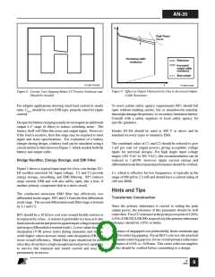
Increasing cable
resistance
Reference
Increased
output cable
resistance
Auto-restart
PI-2961-072202
I
PI-2962-072202
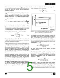
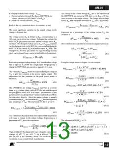
Figure 9. Effect on Output Characteristic Due to Increased Output
Cable Resistance.
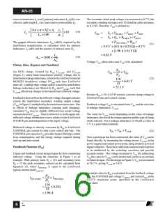
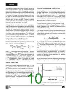
Figure 8. Uneven Core Gapping Makes CC Portion Nonlinear and
Should be Avoided.
For adapter applications drawing rated load current in steady
state, COUT should be a low ESR type, properly rated for ripple
current.
To meet certain safety agency requirements RF1 should fail
open without emitting smoke, fire or incandescent material,
that might damage the primary-to-secondary insulation barrier.
Consult with a safety engineer or local safety agency for
specific guidance.
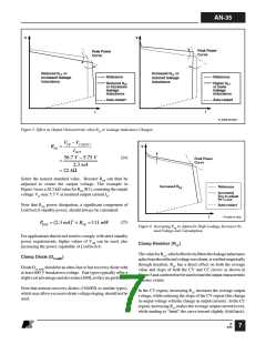
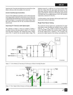
Designsforbatterychargingusuallydonotrequireanadditional
output L-C stage (π filter) to reduce switching noise. The
battery itself will filter this noise and output ripple. However,
if the load is resistive, then this stage may be required to meet
ripple and noise specifications. For evaluation of a battery
charger during design, a battery load can be simulated using a
circuit similar to that shown in Figure 7, which models both the
battery and output cable.
Diodes D1-D4 should be rated at 400 V or above and be
standard recovery types to minimize EMI.
The combined value of C1 and C2 should be selected to give
3 µF per watt (of output power), giving acceptable voltage
ripple for universal designs. For high single input voltage
ranges (185 VAC to 265 VAC), this recommendation can be
reduced to 1 µF/W, however ripple current ratings and
differentialmodelinetransientperformanceshouldbeverified.
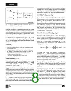
Bridge Rectifier, Energy Storage, and EMI Filter
Figure 1 shows a typical input stage for a low cost design. D1-
D4 rectifies universal AC input voltage. C1 and C2 provide
energy storage, smoothing, and EMI filtering. RF1 reduces
surge current, EMI and will also safely open, like a fuse, if
another primary component fails in a short circuit.
L1, which is effective for low frequencies, is typically in the
range of 680 µH to 2.2 mH and should have a current rating of
≥80 mA RMS.
Hints and Tips
Transformer Construction
The conducted emissions EMI filter has effectively two
differential mode stages. RF1 and C1 form the first differential
mode stage. The second differential mode filter stage is formed
by L1 and C2.
Since the primary inductance is crucial in setting the peak
output power, the tolerance of this parameter should be well
controlled. ForaCCtoleranceatthepeakpowerpointof 20%/
25%(LNK501/LNK500,respectively)theprimaryinductance
tolerance should be 10% or better.
RF1 should be a 10 Ω low cost wire-wound fusible resistor or
be replaced by a fuse. A resistor is preferable to a fuse as it also
limitsinrushcurrentandprotectsagainstinputvoltagetransients
andsurges(differentialornormalmode). Lowervaluesincrease
dissipation (V2/R power term) during transients and inrush,
while higher values increase steady state dissipation (I2R) and
lower overall efficiency. Metal film types should not be used
since they do not have a high enough transient power capability
to survive line transient and inrush current and may fail
prematurely in service.
Tolerance of ungapped core permeability limits minimum gap
size for center leg gapping. For an EE13 core size, the practical
minimum center leg gap size, for an overall primary inductance
toleranceof 10%, is~0.08mm. Thisvarieswithcoresupplier,
so this should be verified before committing to a design.
B
4/03
9

 ETC [ ETC ]