AN-35
capacitorused. Ifanultra-fastdiodehasbeenselected, tryafast
diode as this may allow the snubber to be removed.
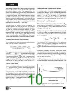
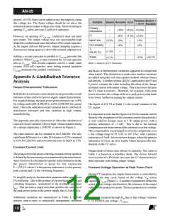
feedback resistor RFB is split into two to form a divider which
limits the voltage across the optocoupler phototransistor. The
optocoupler therefore effectively adjusts the resistor divider
ratiotocontroltheDCvoltageacrossR2andthecurrentintothe
CONTROL pin. For an output tolerance ≤ 5%, VR1 should be
replaced by a reference IC (TL431).
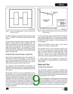
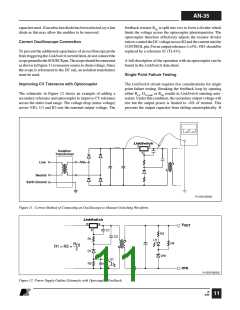
Correct Oscilloscope Connection
To prevent the additional capacitance of an oscilloscope probe
from triggering the LinkSwitch current limit, do not connect the
scopegroundtotheSOURCEpin.Thescopeshouldbeconnected
as shown in Figure 11 to measure source to drain voltage. Since
the scope is referenced to the DC rail, an isolation transformer
must be used.
A full description of the operation with an optocoupler can be
found in the LinkSwitch data sheet.
Single Point Failure Testing
Improving CV Tolerance with Optocoupler
The LinkSwitch circuit requires few considerations for single
point failure testing. Breaking the feedback loop by opening
either RLF, DCLAMP or RFB results in LinkSwitch entering auto-
restart. Under this condition, the secondary output voltage will
rise but the output power is limited to ~8% of normal. This
prevents the output capacitor from failing catastrophically. If
The schematic in Figure 12 shows an example of adding a
secondary reference and optocoupler to improve CV tolerance
across the entire load range. The voltage drop (sense voltage)
across VR1, U1 and R3 sets the nominal output voltage. The
Isolation
Transformer
PI-3164-032403
Figure 11. Correct Method of Connecting an Oscilloscope to Measure Switching Waveform.
LinkSwitch
D
S
V
OUT
C
C1
R3
C2
R1
U1
R4
R
2
FB
R1 = R2 =
D1
R2
VR1
U1
C3
RTN
PI-3222-082202
Figure 12. Power Supply Outline Schematic with Optocoupler Feedback.
B
4/03
11

 ETC [ ETC ]