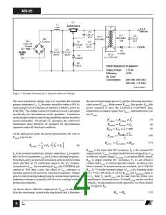
AN-35
cross sectional area Ae (cm2), primary inductance LP (µH), core
effective path length Le (cm) and relative permeability µr:
The secondary diode peak voltage was measured as 0.7 V, the
secondarywindingresistanceas0.15Ωandthecableresistance
as 0.23 Ω. Therefore VSEC is defined as:
2
0.4 ×π × NP × Ae Le
(18)
Lg =
−
×10
VSEC
=
=
VO + VRCABLE + VDOUT + VRSEC
VO + (IO × RCABLE ) + VDOUT
+ (ISEC(PEAK) × RSEC )
LP ×100
µr
The gapped effective inductance ALG (nH/t2), required by the
transformer manufacturer, is calculated from the primary
inductance LP (µH) and the number of primary turns NP:
(21)
= 5.5 V + (0.5 A × 0.23 Ω) + 0.7 V
+ (1.96 A × 0.15 Ω)
= 6.61 V
LP
NP2
(19)
ALG = 1000 ×
Voltage VSEC allows the exact VOR to be calculated:
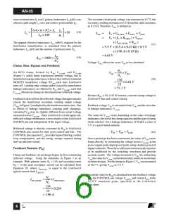
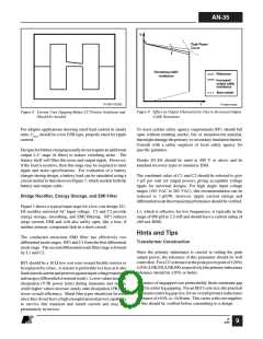
Clamp, Bias, Bypass and Feedback
NP
An RCD clamp, formed by RFB, CCLAMP, and DCLAMP
(Figure 1), safely limits transformer primary voltage, due to
transformerleakageinductance,tobelowtheLinkSwitchinternal
MOSFET breakdown voltage BVDSS each time LinkSwitch
turns off. Leading-edge voltage spikes (caused by transformer
leakage inductance) are filtered by RLF and CCLAMP, such that
CCLAMP effectively charges to the transformer reflected voltage.
VOR =
× VSEC
NS
116
15
(22)
=
× 6.61 V
= 51.1 V
Resistor RFB, a 1%, 0.25 W resistor, converts clamp voltage to
Feedbackisderivedfromthereflectedvoltage,thatapproximates
closely the transformer secondary winding output voltage
(VSEC inFigure1)multipliedbythetransformerturnsratio. Due
to effects of leakage inductance (causing peak charging),
calculated VOR may be slightly different from actual voltage
measured across CCLAMP. Since LinkSwitch is in the upper rail,
reflected voltage information is now relative to the LinkSwitch
SOURCE pin and independent of the input voltage.
LinkSwitch bias and control current.
Feedback voltage VFB is calculated from VOR and the error due
to leakage inductance, VLEAK
.
The value for VLEAK varies depending on the value of leakage
inductance,thesizeoftheclampcapacitorandthetypeofclamp
diode selected. For a leakage inductance of 50 µH, a value of
5 V is a good initial estimate.
Reflected voltage is directly converted by RFB to LinkSwitch
CONTROL pin current for duty cycle control and bias. The
CONTROL pin capacitor CCP provides bypass filtering, control
loop compensation, and the energy storage required during
start-up and auto-restart.
VFB = VOR + VLEAK
(23)
Once a prototype has been constructed, the value of VFB can be
found directly, by measuring the voltage across CCLAMP at the
power supply peak output power point, using a battery powered
digitalvoltmeter. Thesehavesufficientcommonmoderejection
to be unaffected by the switching waveform and provide
accurate results. The voltage measured is VFB. By subtracting
VOR thevalueforVLEAK canbedetermined, usefulasanestimate
in future designs. For the design in Figure 3, VFB was measured
as 56.7 V, giving VLEAK as 5.6 V.
Feedback Resistor (RFB)
Clamp and feedback circuit design begins by first considering
reflected voltage. Using the schematic in Figure 3 as an
example. With primary turns NP = 116 and secondary turns
NS = 15 the peak secondary current can be calculated from
Equation 20, where IPRI(PEAK) is equal to the LinkSwitch
typical current limit ILIM(TYP)
.
An initial value for RFB is calculated from the feedback voltage
VFB, the CONTROL pin voltage VC(IDCT) and current IDCT at the
CC/CV transition point, specified in the LinkSwitch
data sheet.
NP
NS
116
ISEC(PEAK)
=
=
× IPRI(PEAK)
× 0.254
(20)
15
= 1.96 A
B
4/03
6

 ETC [ ETC ]