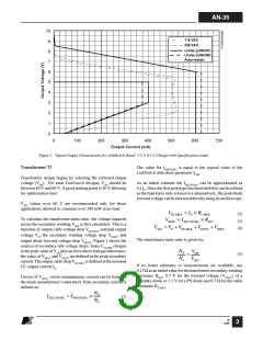
AN-35
U1
L1
1 mH
LinkSwitch
T1
5.5 V,
500 mA
1
4
D
S
5
6
C3
0.22 µF
50 V
C
15 T
#30 AWG
TIW
C5
470 µF
10 V
116 T
#34 AWG
BR1
RF1
10 Ω 1 W
Fusible
1 A, 600 V
C4
0.1 µF
100 V
R1
20.5 kΩ
1%
RTN
3
P
C1
C2
D6
11DQ06
85-265
VAC
4.7 µF
400 V
4.7 µF
400 V
EE13
= 2.55 mH
D5
L
1N4937
R2
100 Ω
PERFORMANCE SUMMARY
Output Power:
Efficiency:
2.75 W
≥72%
No Load
Consumption:
260 mW, 230 VAC
200 mW, 115 VAC
PI-3476-032403
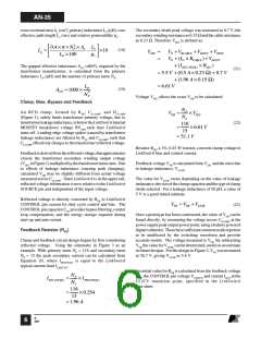
Figure 3. Example Schematic for a Typical LinkSwitch Charger.
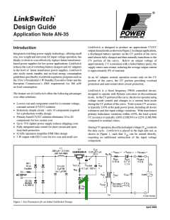
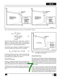
The next transformer design step is to calculate the nominal
primary inductance LP. LP tolerance should be within 10% (to
meet peak power CC tolerance of 20% for LNK501, 25% for
LNK500). The simple LinkSwitch feedback circuit is designed
specifically for discontinuous mode operation. Continuous
mode designs result in control loop instability and are therefore
not recommended. For proper CC operation, the LinkSwitch
transformer must therefore be designed for discontinuous
operation under all line/load conditions.
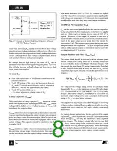
the sum of actual output power PO and the following loss terms:
cable power PCABLE, diode power PDIODE, bias power PBIAS(the
power required to drive the LinkSwitch CONTROL pin),
transformer secondary copper loss PS(CU) , and transformer core
loss PCORE
.
P
= RCABLE × IO2
= VDOUT × IO
(7)
CABLE
(8)
(9)
P
DIODE
P
= VOR × 2.3 mA
BIAS
At the peak power point, the power processed by the core or
PO(EFF) is given by:
KCORE × VE
(10)
(11)
P
=
CORE
2
P
= IS2EC(RMS) × RSEC
2
1
S(CU)
P
=
× LP × IP × fS
(6)
O(EFF)
[
]
2
RCABLE is the total cable DC resistance, IO is the nominal CC
output current, VDOUT is output diode forward voltage drop, VOR
is reflected output voltage, ISEC(RMS) is secondary RMS current,
RSEC is output winding DC resistance, VE is core effective
volume and KCORE is core loss per unit volume. As before, if no
better estimates or measurements are available, use 0.15 Ω for
RSEC, 0.7 V for the forward voltage (VDOUT) of a Schottky diode
or 1.1 V for a PN diode, 0.3 Ω for RCABLE and ISEC(PEAK) equal to
4 x IO. Both VE and KCORE can be read from the ferrite core
manufacturer’smaterialcurves. TofindKCORE,usethecoreflux
swing BM. In discontinuous mode operation, AC Flux Density
BAC is equal to BM:
LP is the nominal transformer primary inductance, IP is equal to
the LinkSwitch parameter ILIM and fS is the switching frequency.
NotethatIP andfS areenclosedinbracketsastheLinkSwitchdata
2
2f
sheet specifies an I f coefficient equal to the IP product,
S
normalized to IDCT. By normalizing to IDCT (the CONTROL pin
current at 30% duty cycle), the effect of IDCT tolerance is
included and does not need to be considered separately. Output
power is therefore dependent primarily on transformer primary
inductance tolerance (typically 10% for low cost high volume
production methods).
As shown above, effective output power PO(EFF) is calculated
from the total energy stored in the transformer and is therefore
(12)
BAC = BM
B
4/03
4

 ETC [ ETC ]