AN-35
During CC operation, duty cycle is controlled by the peak drain
current limit (ILIM). The device current limit is designed to be a
function of reflected voltage such that the load current remains
approximately constant as the load impedance is reduced. When
the output voltage falls to approximately 30% of nominal value
(normally associated with a failed battery), LinkSwitch enters the
auto-restartmodeofoperationtosafelylimitaveragefaultcurrent
(typically 8% of IO).
QUICK START
Figure 1 shows the key parameters and components
needed to generate an initial LinkSwitch design.
Where initial estimates can be used, they are shown
below the parameter they refer to.
1) Let VOR equal 50 V.
With discontinuous mode design, maximum output power is
independentofinputvoltageandisasimplefunctionofprimary
inductance, peak primary current squared and switching
frequency (Equation 6). LinkSwitch controls and cancels out
variationsnormallyassociatedwithfrequencyandpeakcurrent
by specifying a device I2f term. This allows users to easily
design for a specific corner point where CV mode transitions to
CC mode.
2) Define the transformer turns ratio according to
Equation 5. If no better estimates or measure-
ments are available, then let VDOUT equal 0.7 V
foraSchottkyor1.1VforaPNdiode,RCABLE equal
0.3 Ω, RSEC equal 0.15 Ω, ISEC(RMS) equal 2x IO, and
I
SEC(PEAK) equal 4 x IO, where IO is the desired CC
output current and VO is the desired output
voltage at the CV/CC transition point.
Scope
3) Calculate PO(EFF) according to Equation 13. As an
initial estimate for PCORE use 0.1 W.
This application note is for engineers designing an AC-DC
powersupplyusingtheLinkSwitchLNK500orLNK501devices
in a discontinuous mode flyback converter. Since LinkSwitch is
designed to replace linear transformer based power supplies,
the output characteristic provides an approximate CV
characteristic, offering much better line and load regulation
thananequivalentlineartransformer. Theverysimplenatureof
the LinkSwitch circuit allows an initial paper design to be
completed quickly using simple design equations. It is then
recommended that the circuit performance be tuned with a
prototypepowersupplytofinalizeexternalcomponentchoices.
This document therefore highlights the key design parameters
and provides expressions to calculate the transformer turns
ratio,primaryinductanceandclamp/feedbackcomponentvalues.
This enables designers to build an operating prototype and
iterate to reach the final design.
4) Calculate LP according to Equation 14 and
other transformer parameters from Equations
15, 16, 17, 18 and 19.
5) Calculate value for feedback resistor RFB accord-
ing to Equations 20, 21, 22, 23 and 24.
This should be a 1/4 W, 1% part.
6) Set clamp capacitor CCLAMP as a 0.1 µF, 100 V
metalized plastic film type.
7) Set clamp resistor RLF as 100 Ω, 1/4 W.
8) Set CONTROL pin capacitor CCP to be 0.22 µF,
10 V for battery loads or 1 µF, 10 V for resistive
loads.
9) Select input and output components. See
Figure 3 and relevant sections.
For readers who want to generate a design as quickly as
possible, the Quick Start section provides enough information
to generate an initial prototype.
10) Construct prototype.
11) Iterate design (see Hints and Tips section).
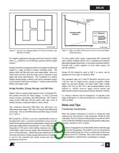
This document does not address transformer construction.
Please see LinkSwitch DAK Engineering Prototype Report for
examplesshowingtypicaltransformerconstructiontechniques.
Further details of support tools and updates to this document
can be found at www.powerint.com.
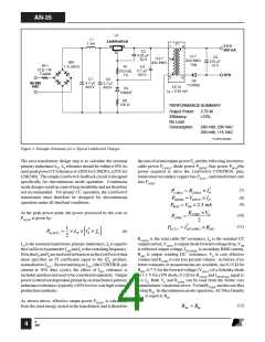
nominalpeakpowerpointoutputvoltageVO,whiletransformer
primary inductance is calculated from the total output power.
Few components require computations, while the balance are
selected from the included recommendations.
CV/CC Circuit Design
The LinkSwitch circuit shown in Figure 3 serves as a CV/CC
chargerexampletoillustratedesigntechniques.Nominaloutput
voltage is 5.5 V and nominal CC output current is 500 mA.
Design and selection criteria for each component are described
startingwiththetransformer. Onceset, transformerparameters
and behavior are used to design clamp, bias and feedback
componentsforpropersupplyoperation. Outputcapacitorsand
the input circuitry can then be determined.
LinkSwitch design methodology is very simple. Transformer
turns ratios and bias component values are selected at the
B
4/03
2

 ETC [ ETC ]