ZENTRUM MIKROELEKTRONIK DRESDEN AG
“ASI for you” IC
Datasheet
Any IC reset or the reception of a Delete_Address call turns the Data Output Register to 0xF and forces the data
output drivers to high impedance state. Simultaneously a Data Strobe is generated, having the same tsetup timing
and tDSR pulse width, as new output data would be driven.
All Data Port operations as well as the generation of a slave response to Data_Exchange (DEXG) requests
depend on the value of Data_Exchange_Disable flag. It becomes set during IC reset or after a Delete_Address
call prohibiting any data port activity after IC initialization or address assignment, as long as the external circuitry
was not pre-conditioned by dedicated parameter output data. The Data_Exchange_Disable flag is cleared while
processing a Write_Parameter (WPAR) request. Consequently the AS-i master has to send a WPAR call in
advance of the first Data_Exchange (DEXG) request in order to enable Data Port operation at the slave.
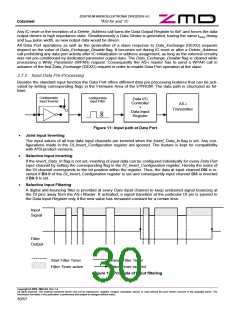
3.7.2 Input Data Pre-Processing
Besides the standard input function the Data Port offers different data pre-processing features that can be acti-
vated by setting corresponding flags in the Firmware Area of the E²PROM. The data path is structured as fol-
lows:
Configurable
Input Inverter
Configurable
Input Filter
Data I/O
Controller
+
AS-i
Transmitter
Data Input
Register
Figure 11: Input path at Data Port
•
•
Joint Input Inverting
The input values of all four data input channels are inverted when the Invert_Data_In flag is set. Any con-
figurations made in the DI_Invert_Configuration register are ignored. The feature is kept for compatibility
with A²SI product versions.
Selective Input Inverting
If the Invert_Data_In flag is not set, inverting of input data can be configured individually for every Data Port
input channel by setting the corresponding flag in the DI_Invert_Configuration register. Hereby the index of
the DI channel corresponds to the bit position within the register. Thus, the data at input channel DI0 is in-
verted if Bit 0 of the DI_Invert_Configuration register is set and consequently input channel DI3 is inverted
if Bit 3 is set.
•
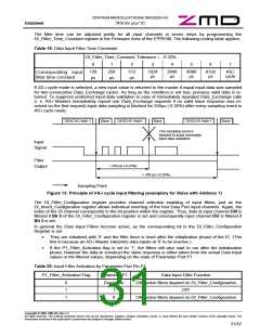
Selective Input Filtering
A digital anti-bouncing filter is provided at every Data Input channel to keep undesired signal bouncing at
the DI pins away from the AS-i Master. If activated, a signal transition at the particular DI pin is passed to
the Data Input Register only if the new value has remained constant for a certain time.
Input
Signal
Filter
Output
Start Filter Timer
Filter Timer active
Reset Filter Timer
Filter Timer expired
Figure 12: Principle of input filtering
Copyright © 2006, ZMD AG, Rev.1.4
All rights reserved. The material contained herein may not be reproduced, adapted, merged, translated, stored, or used without the prior written consent of the copyright owner. The
Information furnished in this publication is preliminary and subject to changes without notice.
30/57

 ZMD [ Zentrum Mikroelektronik Dresden AG ]