ZENTRUM MIKROELEKTRONIK DRESDEN AG
“ASI for you” IC
Datasheet
3.7 Data Port and DSR Pin
3.7.1 Slave Mode
The data port is divided in 4 output and 4 input pins. This makes it possible to control a maximum of 8 binary
devices (4 input + 4 output devices) by a single AS-i Slave IC. Compatibility to multiplexed bi-directional opera-
tion, as it is defined in certain IO Configurations for AS-i Slaves, can be achieved by external connection of cor-
responding DI and DO pins and setting Multiplex_Data flag =’1’ in the Firmware Area of the E²PROM.
Every output pin (DO0…DO3) contains an NMOS open drain output driver; every input pin (DI0…DI3) contains
a high voltage high impedance input stage. Received output data is stored at the Data Output Register and sub-
sequently forwarded to the DO-pins. A certain time (tDI-latch) after new output data was written to the port, the DI-
pins are sampled.
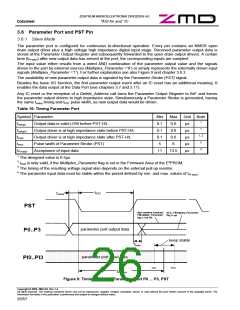
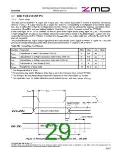
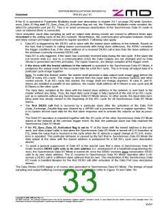
The availability of new output data is signaled by the Data Strobe (DSR) signal as shown in Figure 10. The DSR
pin has an additional reset input function, that is described further in chapter 3.11 IC Reset.
Table 18: Timing Data Port Outputs
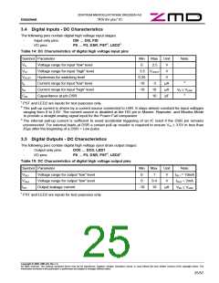
Symbol Parameter
Min
0.1
0.1
0.1
5
Max
0.6
0.6
0.6
6
Unit Note
1
tsetupL
tsetupH
thold
Output data is valid LOW before DSR-H/L
µs
2
Output driver is at high impedance state before DSR-H/L
Output driver is at high impedance state after DSR-H/L
Pulse width of Data Strobe (DSR)
µs
1, 2
µs
3
tDSR
µs
4
tDI-latch
Acceptance of input data
11
13.5
µs
1 The designed value is 0.5µs.
2 Parameter is only valid if Multiplex_Data flag is set in the Firmware Area of the E²PROM.
3 The timing of the resulting voltage signal also depends on the external pull up resistor.
4 The input data must be stable within the period defined by min. and max. values of tDI-latch
.
tDSR
tsetup
DSR
if Multiplex_Data flag
Hi-Z,
Data remains constant,
Multiplex_Data
is set
if
not set
flag is
data port output data
data port input data
DO0..DO3
keep stable
thold
DI0..DI3
max
min
tDI-latch
Figure 10: Timing diagram data port DO0 ... DO3, DI0 … DI3, DSR
Copyright © 2006, ZMD AG, Rev.1.4
All rights reserved. The material contained herein may not be reproduced, adapted, merged, translated, stored, or used without the prior written consent of the copyright owner. The
Information furnished in this publication is preliminary and subject to changes without notice.
29/57

 ZMD [ Zentrum Mikroelektronik Dresden AG ]