<ꢀ5ꢁꢀꢂꢃ<ꢀ.ꢁꢀꢂ
'PJCPEGFꢄ<ꢁꢀꢂꢄ/KETQRTQEGUUQT
ZiLOG
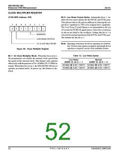
%.1%-ꢄ/7.6+2.+'4ꢄ4')+56'4
ꢌ<ꢁꢀꢂꢄ/27ꢄ#FFTGUUꢄꢁ'*ꢍꢄ
$KVꢄꢈꢆꢄ.QYꢄ0QKUGꢄ%T[UVCNꢄ1RVKQPꢆꢄSetting this bit to 1 en-
ables the low-noise option for the ':6#. and :6#. pins.
This option reduces the gain in addition to reducing the out-
put drive capability to 30% of its original drive capability.
The Low Noise Crystal Option is recommended in the use
of crystalsforPCMCIA applications, where the crystal may
be driven too hard by the oscillator. Setting this bit toꢅ0is
selected for normal operation of the ':6#. and :6#. pins.
The default for this bit is 0.
ꢊ
ꢀ
ꢁ
ꢀ
ꢏ
ꢄ
ꢎ
ꢄ
ꢍ
ꢄ
ꢂ
ꢄ
ꢄ
ꢄ
ꢀ
ꢄꢅ
4'5'48'&
.19ꢅ01+5'ꢅ%4;56#.
:ꢂꢅ%.1%-ꢅ/7.6+2.+'4
0QVGꢅ Operating restrictions for device operation are listed be-
low. If a low-noise option is required, and normal device
operation is required, use the clock multiplier feature.
(KIWTG ꢑꢉꢆ %NQEMꢄ/WNVKRNKGTꢄ4GIKUVGT
6CDNG ꢁꢋꢆ .QYꢄ0QKUGꢄ1RVKQP
$KVꢄꢐꢆꢄ:ꢇꢄ%NQEMꢄ/WNVKRNKGTꢄ/QFGꢆꢄWhen this bit is set to 1,
the programmer can double the internal clock speed from
the speed of the external clock. This feature only operates
effectively withfrequenciesof10–16MHz(20–32MHzin-
ternal). When this bit is set toꢅ0, the Z8S180/Z8L180 device
operates in normal mode. At power-up, this feature is dis-
abled.
.QYꢄ0QKUG
#&&4ꢄꢁ'ꢎꢄDKVꢄꢈꢄꢒꢄꢁ
0QTOCN
#&&4ꢄꢁ'ꢎꢄDKVꢄꢈꢄꢒꢄꢂ
ꢂꢀꢅ/*\ꢅ"ꢅꢎꢑꢏ8ꢇꢅꢄꢀꢀu% ꢍꢍꢅ/*\ꢅ"ꢅꢎꢑꢏ8ꢇꢅꢄꢀꢀu%
ꢄꢀꢅ/*\ꢅ"ꢅꢍꢑꢀ8ꢇꢅꢄꢀꢀu% ꢂꢀꢅ/*\ꢅ"ꢅꢍꢑꢀ8ꢇꢅꢄꢀꢀu%
ꢏꢂ
2ꢅ4ꢅ'ꢅ.ꢅ+ꢅ/ꢅ+ꢅ0ꢅ#ꢅ4ꢅ;
&5ꢀꢀꢁꢀꢀꢂꢃ</2ꢀꢂꢀꢀ

 ZILOG [ ZILOG, INC. ]