<ꢀ5ꢁꢀꢂꢃ<ꢀ.ꢁꢀꢂ
'PJCPEGFꢄ<ꢁꢀꢂꢄ/KETQRTQEGUUQT
ZiLOG
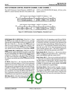
#5%+ꢄ':6'05+10ꢄ%10641.ꢄ4')+56'4ꢄ%*#00'.ꢄꢂꢄ#0&ꢄ%*#00'.ꢄꢁ
The ASCI Extension Control Registers (#5':6ꢀ and
#5':6ꢄ) control functions that have been added to the
ASCIs in the Z8S180/Z8L180 family. All bits in this
register reset to 0.
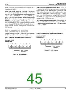
#5%+ꢅ'ZVGPUKQPꢅ%QPVTQNꢅ4GIKUVGTꢅꢀꢅꢈ#5':6ꢀꢅ+ꢌ1ꢅ#FFTGUUꢅꢐꢅꢄꢂ*ꢉ
ꢍ
$KV
ꢊ
ꢁ
ꢏ
ꢎ
ꢂ
ꢄ
ꢀ
&%&ꢀ
%65ꢀ
$4)ꢀ
/QFG
$TGCM
'PCDNG
5GPF
$TGCM
4GUGTXGF
$TGCM
:ꢄ
&KUCDNG &KUCDNG
#5%+ꢅ'ZVGPUKQPꢅ%QPVTQNꢅ4GIKUVGTꢅꢄꢅꢈ#5':6ꢄꢅ+ꢌ1ꢅ#FFTGUUꢅꢐꢅꢄꢍ*ꢉ
ꢊ
ꢁ
ꢏ
ꢎ
ꢍ
ꢂ
ꢄ
ꢀ
$KV
5GPF
$TGCM
$4)ꢄ
/QFG
$TGCM
'PCDNG
4GUGTXGF 4GUGTXGF
:ꢄ
4GUGTXGF
$TGCM
(KIWTG ꢉꢐꢆ #5%+ꢄ'ZVGPUKQPꢄ%QPVTQNꢄ4GIKUVGTUꢎꢄ%JCPPGNUꢄꢂꢄCPFꢄꢁ
&%&ꢂꢄ&KUCDNGꢄꢌ$KVꢄꢈꢎꢄ#5%+ꢂꢄ1PN[ꢍꢆꢄIf this bit isꢅ0, then
the &%&ꢀ pin auto-enables the ASCI0 receiver, such that
when the pin is negated/High, the Receiver is held in a 4'ꢃ
5'6 state. If this bit is 1, the state of the &%&-pin has no
effect on receiver operation. In either state of this bit, soft-
ware can read the state of the &%&ꢀ pin in the 56#6ꢀ reg-
ister, and the receiver interrupts on a rising edge of &%&ꢀ.
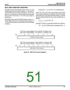
divides 2*+ by 10 or 30, depending on the 25 bit in %06.$,
andfactoredbyapoweroftwo(selectedbythe55ꢂ ꢀ bits),
to obtain the clock that is presented to the transmitter and
receiver and output on the %-# pin. If 55ꢂ ꢀ are not ꢄꢄꢄ,
and this bit is 1, the Baud Rate Generator divides 2*+ by
twice the sum of the 16-bit value (programmed into the
Time Constant registers) and 2. This mode is identical to
the operation of the baud rate generator in the '5%%.
%65ꢂꢄ&KUCDNGꢄꢌ$KVꢄꢑꢎꢄ#5%+ꢂꢄ1PN[ꢍꢆꢄIf this bitisꢅ0,thenthe
%65ꢀ pin auto-enables the #5%+1 transmitter, in that when
the pin is negated/High, the 6&4' bit in the 56#6ꢀ register
is forced to 0. If this bit is 1, the state of the %65ꢀ pin has
no effect on the transmitter. Regardless of the state of this
bit, software can read the state of the %65ꢀ pin the %06.$ꢀ
register.
$TGCMꢄ'PCDNGꢄꢌ$KVꢄꢇꢍꢆꢄIf this bit is 1, the receiver detects
$4'#- conditions and report them in bit 1, and the trans-
mitter sends $4'#-s under the control of bit 0.
$TGCMꢄ&GVGEVꢄꢌ$KVꢄꢁꢍꢆꢄThe receiver sets this read-only bit to
1 when an all-zero character with a Framing Error becomes
the oldest character in the 4Zꢅ(+(1. The bit is cleared when
software writes aꢅ0to the '(4 bit in %06.# register, also
by 4'5'6, by +15612 mode, and for #5%+ꢀ, if the &%&ꢀ
pin is auto-enabled and is negated (High).
:ꢁꢄꢌ$KVꢄꢉꢍꢆꢄIf this bit is 1, the clock from the Baud Rate
Generator or %-# pin is taken as a 1X-bit clock (sometimes
called isochronous mode). In this mode, receive data on the
4:# pin must be synchronized to the clock on the %-# pin,
regardless of whether %-# is an input or an output. If this
bit isꢅ0, the clock from the Baud Rate Generator or %-#
pin is divided by 16 or 64 per the &4 bit in the %06.$ reg-
ister, to obtain the actual bit rate. In this mode, receive data
onthe4:# pin isnot required tobe synchronized to a clock.
5GPFꢄ$TGCMꢄꢌ$KVꢄꢂꢍꢆꢄIf thisbit and bit 2 are both1, the trans-
mitter holds the 6:# pin Low to send a $4'#- condition.
The duration of the $4'#- is under software control (one
of the PRTs or CTCs can be used to time it). This bit resets
toꢅ0, inwhichstate6:# carriesthe serialoutputofthetrans-
mitter.
$4)ꢄ/QFGꢄꢌ$KVꢄꢋꢍꢆꢄIf the 55ꢂ ꢀ bits in the %06.$ register
are not ꢄꢄꢄ, and this bit isꢅ0, the ASCI Baud Rate Generator
&5ꢀꢀꢁꢀꢀꢂꢃ</2ꢀꢂꢀꢀ
2ꢅ4ꢅ'ꢅ.ꢅ+ꢅ/ꢅ+ꢅ0ꢅ#ꢅ4ꢅ;
ꢎꢋ

 ZILOG [ ZILOG, INC. ]