eZ80L92 MCU
Product Specification
131
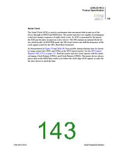
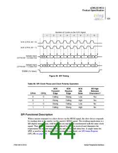
Number of Cycles on the SCK Signal
4 5 6
1
2
3
7
8
SCK (CPOL bit = 0)
SCK (CPOL bit = 1)
Sample Input
(CPHA bit = 0) Data Out
MSB
6
5
4
3
2
1
LSB
Sample Input
(CPHA bit = 1) Data Out
MSB
6
5
4
3
2
1
LSB
Enable (To Slave)
Figure 29. SPI Timing
Table 68. SPI Clock Phase and Clock Polarity Operation
SCK
Transmit
Edge
SCK
Receive
Edge
SCK
Idle
State
SS High
Between
Characters?
CPHA
CPOL
0
0
1
1
0
1
0
1
Falling
Rising
Rising
Falling
Rising
Falling
Falling
Rising
Low
High
Low
High
Yes
Yes
No
No
SPI Functional Description
When a master transmits to a slave device via the MOSI signal, the slave device responds
by sending data to the master via the master's MISO signal. The resulting implication is a
full-duplex transmission, with both data out and data in synchronized with the same clock
signal. Thus the byte transmitted is replaced by the byte received and eliminates the
requirement for separate transmit-empty and receive-full status bits. A single status bit,
SPIF, is used to signify that the I/O operation is completed, see SPI Status Register
(SPI_SR) on page 136.
PS013015-0316
Serial Peripheral Interface

 ZILOG [ ZILOG, INC. ]