eZ80L92 MCU
Product Specification
130
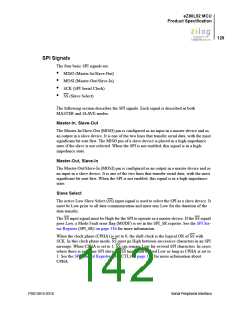
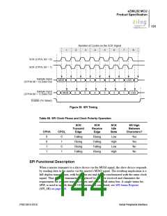
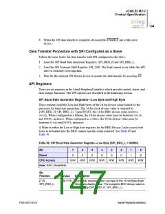
Serial Clock
The Serial Clock (SCK) is used to synchronize data movement both in and out of the
device through its MOSI and MISO pins. The master and slave are capable of exchanging
a data byte during a sequence of eight clock cycles. As SCK is generated by the master,
the SCK pin becomes an input on a slave device. The SPI contains an internal divide-by-
two clock divider. In MASTER mode, the SPI serial clock is one-half the frequency of the
clock signal created by the SPI’s Baud Rate Generator.
As demonstrated in Figure 29 and Table 68, four possible timing relations may be chosen
by using control bits CPOL and CPHA in the SPI Control register. See the SPI Control
Register (SPI_CTL) on page 135. Both the master and slave must operate with the identi-
cal timing, Clock Polarity (CPOL), and Clock Polarity (CPHA). The master device always
places data on the MOSI line a half-cycle before the clock edge (SCK signal), in order for
the slave device to latch the data.
PS013015-0316
Serial Peripheral Interface

 ZILOG [ ZILOG, INC. ]