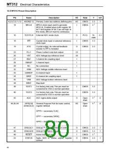
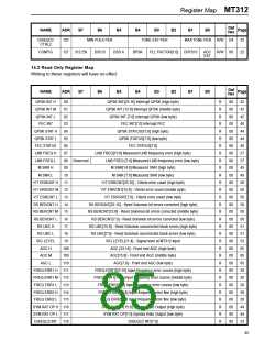
Electrical Characteristics MT312
Note 1.8V tolerant pins with thresholds related to 3.3V.
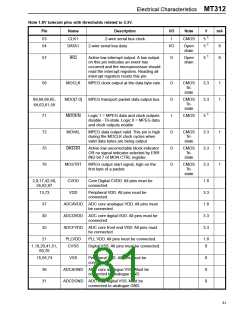
Pin
Name
Description
I/O
Note
V
mA
1
53
54
CLK1
2-wire serial bus clock
I
CMOS
5
5
1
1
DATA1
2-wire serial bus data
I/O
Open
drain
6
6
57
IRQ
Active low interrupt output. A low output
on this pin indicates an event has
O
Open
drain
5
occurred and the microprocessor should
read the interrupt registers. Reading all
interrupt registers resets this pin.
58
MOCLK
MDO[7:0]
MDOEN
MOVAL
MPEG clock output at the data byte rate.
O
O
I
CMOS
Tri-
state
3.3
3.3
1
1
69,68,66,65,
64,63,61,59
MPEG transport packet data output bus.
CMOS
Tri-
state
1
71
72
75
76
Logic 1 = MPEG data and clock outputs
disable - Tri-state. Logic 0 = MPEG data
and clock outputs enable
CMOS
5
MPEG data output valid. This pin is high
during the MOCLK clock cycles when
valid data bytes are being output.
O
O
O
CMOS
Tri-
state
3.3
3.3
3.3
1
1
1
BKERR
Active low uncorrectable block indicator
OR no signal indicator selected by ERR
IND bit 7 of MON CTRL register.
CMOS
Tri-
state
MOSTRT
MPEG output start signal, high on the
first byte of a packet.
CMOS
Tri-
state
2,9,17,42,50,
55,62,67
CVDD
VDD
Core Digital CVDD. All pins must be
connected.
1.8
3.3
1.8
3.3
3.3
13,73
Peripheral VDD. All pins must be
connected.
37
ADCAVDD ADC core analogue VDD. All pins must
be connected.
30
ADCDVDD ADC core digital VDD. All pins must be
connected.
25
ADCFVDD ADC core front end VDD. All pins must
be connected.
21
PLLVDD
CVSS
PLL VDD. All pins must be connected.
Digital VSS. All pins must be connected.
1.8
0
1,10,20,41,51,
60,70
15,56,74
VSS
Peripheral VSS. All pins must be
connected.
0
0
0
36
ADCAGND ADC core analogue VSS. Must be
connected to analogue GND.
31
ADCDGND ADC core digital VSS. Must be
connected to analogue GND.
81

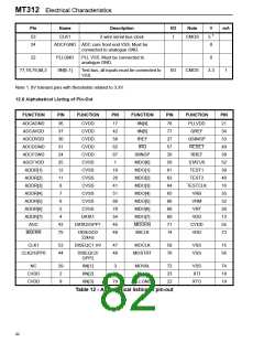
 ZARLINK [ ZARLINK SEMICONDUCTOR INC ]