MT312 Electrical Characteristics
12 Electrical Characteristics
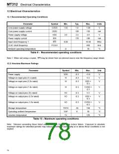
12.1 Recommended Operating Conditions
Parameter
Symbol
Min.
Typ.
Max.
Units
Core power supply voltage
Core power supply current
Power supply voltage
CVDD
CIDD
VDD
1.62
1.8
130
3.3
1.98
150
3.6
V
mA
V
3.0
9.99
0
Power supply current
IDD
170
180
16.00
450
70
mA
MHz
kHz
°C
Input clock frequency 1
CLK1 clock frequency
XTI
FCLK1
Ambient operating temperature
Table 9 - Recommended operating conditions
Note 1. When not using a crystal, XTI may be driven from an external source over the frequency range shown.
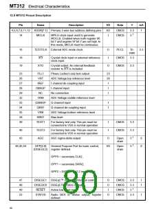
12.2 Absolute Maximum Ratings
Parameter
Symbol
Min.
Max.
Unit
Power supply
VDD
VI
-0.3
-0.3
-0.3
+3.6
5.5
V
V
V
Voltage on input pins (5 v rated)
Voltage on input pins (3.3v rated)
VI
VDD +
0.3
Voltage on input pins (1.8v rated)
VI
-0.3
CVDD +
0.3
V
Voltage on output pins (5v rated)
Voltage on output pins (3.3v rated)
VO
VO
-0.3
-0.3
5.5
V
V
VDD +
0.3
Voltage on output pins (1.8v rated)
VO
-0.3
CVDD +
0.3
V
Storage temperature
TSTG
TOP
TJ
-55
0
150
70
°C
°C
°C
Operating ambient temperature
Junction temperature
125
Table 10 - Maximum operating conditions
Note: Stresses exceeding these listed under ’Absolute Ratings’ may induce failure. Exposure to absolute
maximum ratings for extended periods may reduce reliabilty. Functionality at or above these conditions is not
implied.
78

 ZARLINK [ ZARLINK SEMICONDUCTOR INC ]