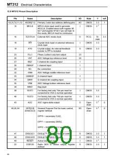
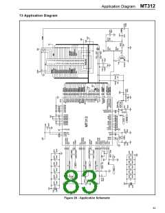
MT312 Electrical Characteristics
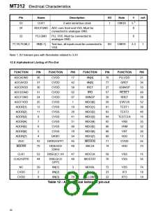
12.5 MT312 Pinout Description
Pin
Name
Description
I/O
Note
V
mA
4,5,6,7,8,11,12 ADDR[7:1] Primary 2-wire bus address defining pins
I/O
I
CMOS
CMOS
3.3
1
1
14
MICLK
MPEG clock input used to generate
MOCLK. Enabled when both register 96
bit 7 and register 97 bit 7 are set high. In
this mode, MICLK must be continuous.
5
16
18
19
TESTCLK
XTI
External ADC mode clock.
O
I
PECL
CMOS
CMOS
Tri-
state
3.3
Crystal clock input or external reference
clock input.
3.3
3.3
XTO
Crystal output. An internal feedback
resistor to XTI is included
O
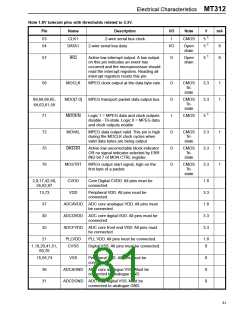
23
26
27
28
29
32
33
34
35
38
39
PLL1
VRT
Phase Locked Loop test output
ADC Voltage top reference level
I channel de-coupling input
I channel input
23
26
IREF
I
I
I
ISINGP
NC
No connection
VRM
ADC Voltage middle reference level
Q channel input
QSINGP
QREF
VRB
I
I
Q channel de-coupling input
ADC Voltage bottom reference level
Bias level
RREF
TEST1
For factory test only. This pin must be
connected to VSS in normal operation
I
I
CMOS
CMOS
3.3
3.3
40
43
TEST2
AGC
For factory test only. This pin must be
connected to VSS in normal operation
1
AGC sigma-delta output
O
I/O
Open
drain
5
6
6
1
46,45,44
GPP[2:0]
(DISEQC2) register defined.
General Purpose Port for tuner control,
Open
drain
5
GPP0 = secondary CLK2,
GPP1 = secondary DATA2,
GPP2 = DiSEqC™ v2.2 input signal.
47
48
49
52
DISEQC1
DISEQC0
RESET
DiSEqC™ Horizontal/Vertical control
DiSEqCTM 22kHz output
O
O
I
CMOS
CMOS
CMOS
CMOS
3.3
3.3
1
1
1
Active low reset input
5
STATUS
Audio BER or Status output, register
O
3.3
1
defined
80

 ZARLINK [ ZARLINK SEMICONDUCTOR INC ]