Le77D11
Data Sheet
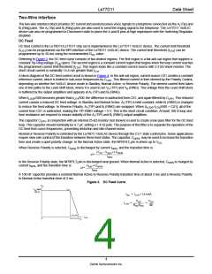
where 2 • RF is the total resistance of the external fuse resistors in the circuit, RIMT is the impedance setting resistor, KOUT is the
gain from VOUT to VAB, and KV is the voice current gain defined in the Transmission Specifications Table. Note that the equation
reveals that Z2WIN is a function of the selectable resistors, RIMT and RF. For example, if RF = 0 Ω and RIMT is 100 k, the terminating
impedance is 600 Ω. This is the configuration used in this data sheet for defining the device specifications. However, in a real
application, RF = 50 Ω is recommended, producing a total input impedance of 700 Ω which is a good starting point for meeting
worldwide requirements using the programmable filters of the Le78D11 VoSLAC device.
Two-Wire to Four-Wire Gain (G )
24
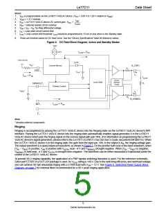
The two-wire to four-wire gain is the gain from the phone line to the VOUT output of the Le77D11 VoSLIC device. To solve for
G24, the VIN pin is grounded (see Figure 7).
VOUT
VAB
1
------------- = G24 = -----------------------------------------
2RF
-------------------- + KOUT
KVRIMT
or
2RF
KVRIMT
G24 = –20log KOUT + -------------------- in dB
Using the values of RIMT and RF from the application example, G24 for this circuit is –10.9 dB.
Four-Wire to Two-Wire Gain (G )
42
G42 is the gain from the VIN input to the line. This gain is defined as VAB/VIN.
RL
------------------------
K
IN
F
VAB
RL + 2R
--------------------------------------------------
--------- = G 42
VIN
=
K
OUTRIMTKV
1 + ----------------------------------
RL + 2RF
or
RL
------------------------
K
IN
F
RL + 2R
--------------------------------------------------
G42 = –20log
in dB
K
OUTRIMTKV
1 + -----------------------------------
RL + 2RF
where KIN is the gain from VIN to VAB. Using the values of RIMT and RF from the application example and RL = 600 Ω, G42 for
this circuit is 7.3 dB.
Note:
Equation derivations can be found in the Zarlink Le77D11/Le78D11 Chip Set User’s Guide (document ID# 080716).
Figure 7. Transmission Block Diagram
Ai
RF*
RS
VINi
CFILT
VHPi
VOUTi
i
Sense
Kv
VAB
RL*
IL
CHPi
*
RIMTi*
RS
RF*
Bi
Note:
* denotes external components
8
Zarlink Semiconductor Inc.

 ZARLINK [ ZARLINK SEMICONDUCTOR INC ]