Le77D11
Data Sheet
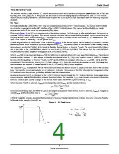
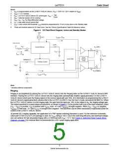
Notes:
1. DC is programmable via the Le78D11 VoSLAC device. (VDC = 0.00 V to 1.20 V relative to VREF.)
2. VREF = 1.4 V nominal.
V
IIMT
DC = Le77D11 VoSLIC device DC current gain. KDC = -------------- .
3.
4.
K
R
ILOOP
DC = external resistor 20 kΩ nominal.
5. VAB = VAi – VBi Tip-Ring differential voltage.
6.
7.
I
I
SC = Loop short circuit current limit.
LTH = Loop current limit threshold. ILTH should be programmed to 15 mA or less when in the Standby state.
8. These are nominal values for DC feed curve. See the "Device Specifications" table for tolerance values.
Figure 4. DC Feed Block Diagram, Active and Standby Modes
VCC
CS1
ILOOP KDC
VDC SLAC
LPFi
RDC
*
Current Mirrors
Ai (TIP)
RS
RDCi
CLPFi
*
IA
ILTH KDC
ILOOP
Sum/
Sense/
Fault
Level Shift
RL
NPRFILT i
Polarity Control
CNPRi
*
IB
RS
Bi (RING)
ILOOP KDC
IMTi
Fi
Note:
* denotes external components
Ringing
Ringing is accomplished by placing the Le77D11 VoSLIC device into the Ringing state via the Le78D11 VoSLAC device's MPI
interface. Placing the Le77D11 VoSLIC device into the ringing state automatically enables signal generator A in the Le78D11
VoSLAC device which puts the ringing signal on the receive signal path (pin VIN). (For information on programming the Le78D11
VoSLAC device's signal generators, please refer to the Le77D11 /Le78D11 Chip Set User’s Guide, document ID# 080716). When
the Le77D11 VoSLIC device is in the ringing state, the gain from the input pin, VIN, to the output is KR, the ringing voltage gain.
The output waveform is a quasi-balanced waveform, as shown in Figure 5. On the positive half cycle of the input waveform, when
(VIN – VREF) is positive, VAB is positive with VA(TIP) near –4 V and VB(RING) brought negative. When (VIN – VREF) is negative,
VB(RING) is held near –4 V and VA(TIP) is brought more negative. The waveform can be either sinusoidal or trapezoidal under the
control of the Le78D11 VoSLAC device.
To provide 90-V ringing capability, the application of a PNP bipolar switching transistor is used. For the reference schematic,
Zetex part FZT955 in a SOT-223 package is used. Its VCEO rating is 140 V. Due to the switching efficiency and overhead voltage,
one can achieve 90 Vpk sinusoidal ringing with a 5 REN load with VSW = 12 V. See Figure 6, Switching Power Supply Block
Diagram, on page 7 for external filters recommended for a 90-V peak ringing application.
5
Zarlink Semiconductor Inc.

 ZARLINK [ ZARLINK SEMICONDUCTOR INC ]