Le77D11
Data Sheet
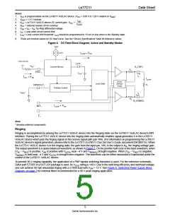
Fault Detection
Each channel of the Le77D11 Dual VoSLIC device has a fault detection pin, F1 or F2. These pins are driven low when a
longitudinal current fault or foreign voltage fault occurs (see Figure 4, DC Feed Block Diagram, Active and Standby Modes, on
page 5). When not in Disconnect state, there are three conditions that will cause the Fi pin to indicate a fault condition:
•
•
•
|IA − IB| > ILONG
In Normal Active and Standby state, a foreign voltage fault occurs in which VA is above ground or VB is close to VREG
In Reverse Polarity state, a foreign voltage fault occurs in which VB is above ground or VA is close to VREG
.
.
In the Disconnect state, fault detection is not supported; however, fault conditions can be monitored by the Le78D11 device.
For more details on AC, DC fault detection, loss of power, or clock-failure alarm, please refer to the Zarlink Le77D11/Le78D11
Chip Set User’s Guide (document ID# 080716).
Signal Conditioning
The RDCi pin is used to set the DC feed current limit, as described in the DC feed section.
The IMTi pin provides KDC times the loop current to the Le78D11 VoSLAC device. The Le78D11 VoSLAC device implements all
loop supervision and ring trip processing on this signal.
I
A + IB
2
---------------
IIMT
=
• KDC
Thermal Overload
When the die temperature around the power amplifier of an Le77D11 Dual VoSLIC device channel reaches approximately 160°C,
the IMT pin of that channel is pulled High. At the same time, all the blocks controlling that channel of the device are shut off,
except for the logic interface block. The VoSLIC channel goes into a state similar to Disconnect, making the line current zero.
When the temperature drops below 145°C, the VoSLIC channel returns to its previous state. It is important to recognize that even
while a channel experiences thermal overload, the state of the device can be modified. At TSD, the switcher is turned off.
Control Logic
Each channel of the Le77D11 VoSLIC device has three input pins from the Le78D11 VoSLAC device (C3, C2, and C1). The inputs
set the operational state of each channel. There are six operational VoSLIC device states (See Table 1): Low Power Standby,
Disconnect, Normal Active, Reverse Polarity, Ringing and Line Test. This leaves two reserved logic states.
Table 1. Device Operating States
C3
C2
C1
Operating Mode
Description
Voice transmission disabled. Maximum loop current capability and loop
current sensing range are reduced.
0
0
0
Low Power Standby
Le77D11 Dual VoSLIC device channel is shut down and switching power
supply is shut off.*
Le77D11 Dual VoSLIC device channel fully operational. Ai (TIP) is more
positive than Bi (RING). Also used for on-hook transmission.
0
0
0
1
1
0
Disconnect
Normal Active
Similar to normal active, but DC polarity is reversed so that the Bi (RING)
lead is more positive than the Ai (TIP) lead. Also used for on-hook
transmission.
0
1
1
Reverse Polarity
Ringing state with VAB set to KR • VIN. The switching supply maintains
minimum headroom for the sourcing and sinking amplifiers in order to
maximize power efficiency.
Similar to ringing state with reduced bias currents for lower noise. Loop
current sensing range is limited. See IMT pin specifications.
1
1
0
0
0
1
Ringing
Line Test State
1
1
1
1
0
1
Reserved
Reserved
Not used.
Not used.
Note:
* When in Disconnect state, the DC-DC converter is disabled and the VREG voltage will decay to 0 V. The Ai and Bi outputs are disabled; however,
they still have ESD protection diodes to BGND and VREG which will provide a low impedance clamp to any line voltages >± 0.5 V.
*When transitioning from any state to Disconnect, the Le77D11 device momentarily passes through Reverse Polarity, pulling the A-lead towards
Vreg. During line testing, when the SLIC device is placed in the Disconnect state, wait >3 seconds before proceeding with line measurements.
9
Zarlink Semiconductor Inc.

 ZARLINK [ ZARLINK SEMICONDUCTOR INC ]