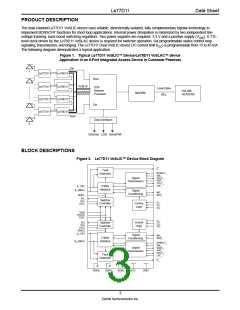
Le77D11
Data Sheet
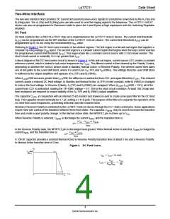
For this application, RBD is 180 Ω and capacitor CBD is 27 nF to increase the switching speed and efficiency. This increases the
power available during the Ringing state when the converter operates at the highest currents. The capacitors CFL and CVREG use
very low ESR film capacitors to minimize ripple and noise on VREG. The capacitance is sized to permit more rapid charging of the
capacitors, and hence a faster slew rate. Reduction of switcher noise is accomplished by using lower ESR capacitors and
increasing the value of the LVREG inductor in the post filter. The power supply output is able to track the ringing waveform under
these conditions.
Figure 6. Switching Power Supply Block Diagram
VSW
Inside Le77D11 SLIC Device
-
CSW
CSWi
*
+
VSW
BGND
+
LEADING
EDGE
BLANKING
FILTER
VCC
0.28 V
-
RLIMi
*
LATCH
+
-
48 V
800 K
OUTPUT
RESET
SET
ILSi
In Active
8 V
800 K
I=
100 Vin
800 K
in Active
15 V
800 K
In Ringing
CBDi
*
VREF
I=
DD2
*
1.4 V
CLAMP
in Ringing
VSW
QSWi
*
DRIVER
RBDi
*
-
SDi
+
CHSi
COMPARATOR
DSWi
CFLi
*
TRIANGLE
WAVE
CHSi
*
*
*
LSWi
*
FSET
RRAMP
BGND
BGND
CHCLK
10% High Duty Cycle
85.3 kHz or 256 kHz
Selectable via the Le78D11 device
800 k
LVREGi
*
CVREGi
*
CVREGi
*
CESRi*
VREGi
BGND
BGND
Note:
* denotes external components
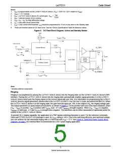
Signal Transmission
In Normal Active and Reverse Polarity states, the AC line current is sensed across the internal resistors, RS (see Figure 7,
Transmission Block Diagram, on page 8), summed, attenuated and converted to voltage at the CFILT pin. This voltage then goes
through a high pass filter (with a nominal 13 Hz corner frequency), implemented using an on-chip 8 kΩ nominal resistor and an
external CHP capacitor, is amplified, and sent to the Le78D11 VoSLAC device at the VOUT pin. The output is proportional to the
AC metallic component of the line voltage. Additionally, the signal transmission block receives the analog signal from the
Le78D11 VoSLAC device. The analog signal is amplified and sent to the line.A proportion of the signal at VOUT is also fed back
to the line.
There are three parameters which define the AC characteristics of the Le77D11 VoSLIC device. First is the input impedance
presented to the line or two-wire side (Z2WIN), second is the gain from the four-wire (VIN) to the two-wire (VAB) side (G42), and
third is the gain from the two-wire side to the four-wire (VOUT) side (G24).
Input Impedance (Z
)
2WIN
Z2WIN is the impedance presented to the line at the two-wire side, and is defined by:
Z2WIN = 2RF + KVKOUTRIMT
7
Zarlink Semiconductor Inc.

 ZARLINK [ ZARLINK SEMICONDUCTOR INC ]