Le77D11
Data Sheet
Two-Wire Interface
The two-wire interface block provides DC current and sends/receives voice signals to a telephone connected via the Ai (Tip) and
Bi (Ring) pins. The Ai (Tip) and Bi (Ring) pins are also used to send the ringing signal to the telephone. The Le77D11 VoSLIC
device can also be programmed in Disconnect state to place the A and B pins at high impedance with the Switching Regulator
disabled.
DC Feed
DC feed control in the Le78D11/Le77D11 chip set is implemented in the Le77D11 VoSLIC device. The current limit threshold
(ILTH) can be programmed via the MPI interface of the Le78D11 VoSLAC device. The current limit threshold (ILTH) can be
programmed up to 30 mA using the recommended RDC value.
Referring to Figure 3, the DC feed curve consists of two distinct regions. The first region is a flat anti-sat region that supplies a
constant Tip-Ring voltage (VAB open). The second region is a constant current region that begins when the loop current reaches
the programmed current limit threshold (ILTH). This region looks like a constant current source with 3.2 kΩ shunt resistor. The
short circuit current is nominally 14.4 mA greater than ILTH
.
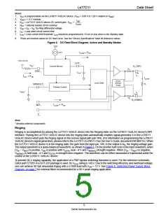
A block diagram of the DC feed control circuit is shown in Figure 4. In the anti-sat region, current source CS1 creates a constant
reference current, which is limited to sub-voice frequencies by CLPFi. This filtered current is then steered by the Polarity Control,
depending on whether the VoSLIC device mode is Standby, Normal Active, or Reverse Polarity. The steered current then takes
one of two paths to the Level Shift block, where it is used to set VA (TIP) and VB (RING). This voltage from the Level Shift block
is buffered by the output amplifiers and appears at Ai (TIP) and Bi (RING).
When ILOOP/500 becomes greater than ILTH/500, the difference is subtracted from CS1, and again filtered by CLPFi. This reduced
current causes a reduced DC feed voltage. In Standby and Normal Active, Ai (TIP) is held constant, while Bi (RING) is changed
to reduce the feed voltage. In Reverse Polarity, Ai (TIP) and Bi (RING) are swapped. When (ILOOP-ILTH)/500 = CS1], all of the
current from CS1 is subtracted, making the TIP-RING voltage = 0 V. This is the short circuit condition. At least 100 Ω loop and
fuse resistance are required to ensure stability of the Ai (TIP) and Bi (RING) output amplifiers.
The capacitor CLPFi, in conjunction with an internal 25-kΩ resistor (not shown) is used to create a low pass filter for the DC feed
loop. This capacitor should nominally be 4.7 µF, setting a 1.4 Hz pole. The purpose of this filter is to separate the operation of the
DC feed from voice frequencies, preventing distortion and idle-channel noise.
Normal or Reverse Polarity is controlled by the Le78D11 VoSLAC device through the C3-1 state control pins. Some applications
require slew rate control of the transition between these feed states. The capacitor, CNPRi, may be used to increase the transition
time and create a quiet polarity change. In the Normal Active state, the NPRFILTi pin is driven up to VCC
.
When Reverse Polarity is selected, CNPRi is discharged by current INPR, and the transition time is:
(VCC – VREF) • CNPRi
∆t= ---------------------------------------------------------
INPR
In the Reverse Polarity state, the NPRFILTi pin is discharged near ground. When Normal Active is selected, CNPRi is charged by
current INPR, and the transition time is:
VREF • CNPRi
∆t= -----------------------------------
INPR
A 100-nF capacitor provides a nominal Normal Active to Reverse Polarity transition time of about 5 ms and a Reverse Polarity
to Normal Active transition time of 3 ms.
Figure 3. DC Feed Curve
VAB
ILTH
VAB open
(48 V)
ISC = ILTH + 14.4mA
VDC
ILTH = ---------------------- = ----------
RDCKDC 40
VDC
14.4 mA
ILOOP
0
ISC
4
Zarlink Semiconductor Inc.

 ZARLINK [ ZARLINK SEMICONDUCTOR INC ]