Le58083
Data Sheet
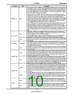
Symbol
Parameter Descriptions
Min
Typ
Max
Unit
Note
Digital Input capacitance
CI
Pins connected to one channel group
10
20
6
Pins connected to both channel groups
pF
Digital Output capacitance
CO
Pins connected to one channel group
10
20
6
Pins connected to both channel groups
Power supply rejection ratio (1.02 kHz, 100 mVRMS, either
path, GX = GR = 0 dB)
PSRR
40
dB
Notes:
1. The CD1, CD2, C3–C7 outputs are resistive for less than a 0.8 V drop. Total current must not exceed absolute maximum ratings.
2. When the digitizer saturates, a resistor of 50 kΩ ± 20 kΩ is connected either to AGND or to VCCA as appropriate to discharge the coupling
capacitor.
3. When the Le58083 Octal SLAC device is in the Inactive state, the analog output will present either a VREF DC output level through a 15
kΩ resistor (VMODE = 0) or a high impedance (VMODE = 1).
4. If there is an external DC path from VOUT to VIN with a gain of GDC and the AISN has a gain of hAISN, then the output offset will be multiplied
by 1 / [1 – (hAISN • GDC)].
5. Power dissipation in the Inactive state is measured with all digital inputs at VIH = VCCD and VIL = DGND and with no load connected to
VOUTC_X pins.
6. The PCM/GCI pins (DRA/DD, DRB, DXA/DU, DXB, FS/FSC, PCLK/DCL, TSCA and TSCB) connect to both four-channel groups and have
double the capacitance and leakage. Also, RST is in this category.
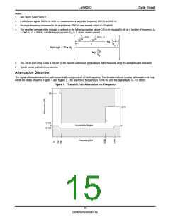
Transmission Characteristics
Table 2. 0 dBm0 Voltage Definitions with Unity Gain in X, R, GX, GR, AX, and AR
Transmit
Transmit
Signal at Digital Interface
(DGIN = 0)
(DGIN = 1)
Receive
0.5024
0.4987
0.5024
Unit
A-law digital mW or equivalent (0 dBm0)
µ-law digital mW or equivalent (0 dBm0)
±22,827 peak linear coded sine wave
0.7804
0.7746
0.7804
0.5024
0.4987
0.5024
Vrms
When relative levels (dBm0) are used in any of the following transmission specifications, the specification holds for any setting
of the GX gain from 0 dB to 12 dB, the GR loss from 0 dB to 12 dB, and the input attenuator (GIN) on or off.
Description
Test Conditions
Min
Typ
Max
Unit
Note
0 dBm0, 1014 Hz
AX = AR = 0 dB
0 to 85° C
–0.25
–0.30
+0.25
+0.30
–40° C
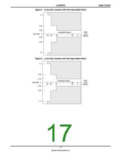
Gain accuracy, D/A or A/D
AX = +6.02 dB and/or
AR = –6.02 dB
0 to 85° C
–0.30
–0.40
+0.30
+0.40
dB
–40° C
Gain accuracy digital-to-digital
Gain accuracy analog-to-analog
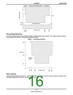
Attenuation distortion
–0.25
–0.25
–0.125
+0.25
+0.25
+0.125
–46
300 Hz to 3 kHz
1
2
Single frequency distortion
Second harmonic distortion, D/A GR = 0 dB
–55
Idle channel noise
Digital looped backweighted
Analog out
Digital out
–68
–55
–78
12
–68
16
dBm0p
dBm0
dBm0p
dBrnc0
dBm0p
dBrnc0
3
3
unweighted
Digital input = 0 A-law
3
Digital input = 0 µ-law
0
0
3, 6
3
3, 6
Analog V = 0 VACA-law
IN
Analog V = 0 VAC µ-law
IN
Crosstalk TX to RX
same channel RX to TX
0 dBm0
0 dBm0
300 to 3400 Hz
300 to 3400 Hz
–75
–75
dBm0
0 dBm0
Crosstalk between channels
SLIC device imped. < 5000 Ω
1014 Hz, Average
dBm0
µs
4
5
TX or RX to TX
TX or RX to RX
End-to-end group delay
–76
–78
678
1014 Hz, Average
B = Z = 0; X = R = 1
14
Zarlink Semiconductor Inc.

 ZARLINK [ ZARLINK SEMICONDUCTOR INC ]