Le58083
Data Sheet
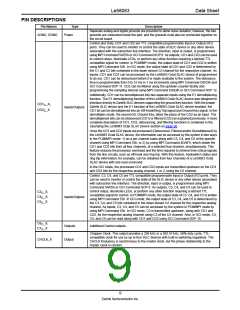
ELECTRICAL CHARACTERISTICS
Typical values are for TA = 25º C and nominal supply voltages. Minimum and maximum values are over the temperature and
supply voltage ranges shown in Operating Ranges, except where noted.
Symbol
VIL
VIH
Parameter Descriptions
Digital Input Low voltage
Digital Input High voltage
Min
Typ
Max
0.8
Unit
Note
V
2.0
Digital Input leakage current
Pins connected to one channel group
0 < V < VCCD
–7
+7
IIL
Otherwise
–120
+180
µA
6
Pins connected to both channel groups
0 < V < VCCD
Otherwise
–14
–240
+14
+360
VHYS
Digital Input hysteresis
0.16
0.25
0.34
V
V
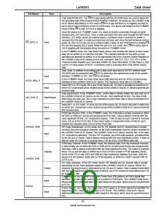
Digital Output Low voltage
CD1–C7 (IOL = 4 mA)
0.4
0.8
0.4
0.4
CD1–C7 (IOL = 8 mA)
TSCA/ TSCB (IOL =14 mA)
Other digital outputs (IOL = 2 mA)
VOL
1
1
Digital Output High voltage
CD1–C7 (IOH = 4 mA)
V
CCD – 0.4 V
VOH
V
CD1–C7 (IOH = 8 mA)
Other digital outputs (IOH = 400 µA)
VCCD – 0.8 V
2.4
Digital Output leakage current (Hi-Z state)
Pins connected to one channel group
0 < V < VCCD
–7
+7
IOL
Otherwise
–120
+180
µA
6
Pins connected to both channel groups
0 < V < VCCD
Otherwise
–14
–240
+14
+360
Input attenuator gain
GIN
VIR
DGIN = 0
0.6438
1
V/V
Vpk
DGIN = 1
Analog input voltage range (Relative to VREF)
AX = 0 dB, attenuator on (DGIN = 0)
±1.584
±0.792
±1.02
AX = 6.02 dB, attenuator on (DGIN = 0)
AX = 0 dB, attenuator off (DGIN = 1)
AX = 6.02 dB, attenuator off (DGIN = 1)
±0.51
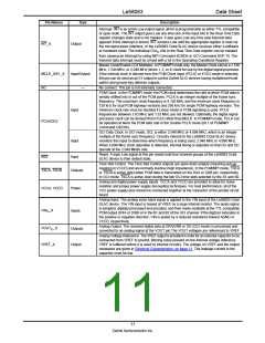
VIOS
ZIN
Offset voltage allowed on VIN
Analog input impedance to VREF, 300 to 3400 Hz
Current into analog input for an input voltage of 3.3 V
Current out of analog input for an input voltage of –0.3 V
VOUT output impedance
Allowable capacitance, VOUT to AGND
–50
600
50
50
1400
115
130
10
500
4
1.57
130
mV
kΩ
I
2
2
IP
µA
I
50
IN
ZOUT
CLOUT
IOUT
VREF
ZREF
1
Ω
pF
mApk
V
–4
1.43
70
3
VOUT output current (F< 3400 Hz)
VREF_X output open circuit voltage (leakage < 20 nA)
VREF_X output impedance (F <3400 Hz)
1.5
kΩ
VOUT analog output voltage range (Relative to VREF)
±1.02
±0.51
VOR
AR = 0 dB
Vpk
mV
V/V
AR = −6.02 dB
VOUT offset voltage (AISN off)
VOUT offset voltage (AISN on)
VOOS
VOOSA
–40
–80
40
80
4
5
AISN gain - expected gain (input = 0 dBm0, 1014 Hz)
Attenuator on (DGIN = 0)
GAISN
–0.010
–0.016
0.010
0.016
Attenuator off (DGIN = 1)
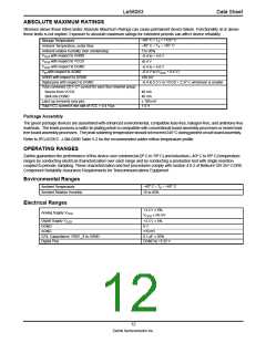
Power dissipation
All channels active
1 channel active
260
55
26
340
100
36
PD
mW
All channels inactive
13
Zarlink Semiconductor Inc.

 ZARLINK [ ZARLINK SEMICONDUCTOR INC ]