Le58083
Data Sheet
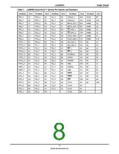
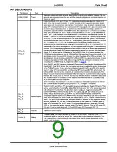
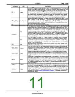
Pin Names
Type
Description
Interrupt. INT is an active Low output signal, which is programmable as either TTL-compatible
or open drain. The INT output goes Low any time one of the input bits in the Real Time Data
register changes state and is not masked. It also goes Low any time new transmit data
appears if this interrupt is armed. INT remains Low until the appropriate register is read via
the microprocessor interface, or the Le58083 Octal SLAC device receives either a software
INT_X
Output
or hardware reset. The individual CDx bits in the Real Time Data register can be masked
C
from causing an interrupt by using MPI Command 6C/6Dh or GCI Command SOP 14. The
transmit data interrupt must be armed with a bit in the Operating Conditions Register.
Master Clock/Enable CD1 Multiplex. In PCM/MPI mode only, the Master Clock can be a 1.536
MHz, 1.544 MHz, or 2.048 MHz (times 1, 2, or 4) clock for use by the digital signal processor.
If the internal clock is derived from the PCM Clock Input (PCLK) or if GCI mode is selected,
this pin can be used as an E1 output to control Zarlink SLIC devices having multiplexed hook
switch and ground key detector outputs.
MCLK_X/E1_X
NC
Input/Output
—
No connect. This pin is not internally connected.
PCM Clock. In the PCM/MPI mode, the PCM clock determines the rate at which PCM data is
serially shifted into or out of the PCM ports. PCLK is an integer multiple of the frame sync
frequency. The maximum clock frequency is 8.192 MHz and the minimum clock frequency is
128 kHz for dual PCM highway versions and 256 kHz for single PCM highway versions. The
minimum clock rate must be doubled if Linear mode or PCM signaling is used. PCLK
frequencies between 1.03 MHz and 1.53 MHz are not allowed. Optionally, the digital signal
processor clock can be derived from PCLK rather than MCLK. In PCM/MPI mode, PCLK can
be operated at twice the PCM data rate in the Double PCLK mode (bit 1 of PCM/MPI
Command C8/C9h).
GCI Data Clock. In GCI mode, DCL is either 2.048 MHz or 4.096 MHz, which is an integer
multiple of the frame sync frequency. Circuitry internal to the Le58083 Octal SLAC device
monitors this input to determine which frequency is being used, 2.048 MHz or 4.096 MHz.
When 4.096 MHz clock operation is detected, internal timing is adjusted so that DU and DD
operate at the 2.048 Mbit/s rate.
Input
Input
PCLK/DCL
Reset. A logic Low signal at this pin resets both four-channel groups of the Le58083 Octal
SLAC device to their default state.
Input
RST
Time Slot Control. The Time Slot Control outputs are open-drain outputs (requiring pull-up
resistors to VCCD) and are normally inactive (high impedance). In the PCM/MPI mode, TSCA
or TSCB is active (low) when PCM data is transmitted on the DXA or DXB pin, respectively.
In GCI mode, TSCA is active (low) during the two GCI time slots selected by the S1 and S0.
TSCA, TSCB
Outputs
Analog and digital power supply inputs. VCCA and VCCD are provided to allow for noise
isolation and proper power supply decoupling techniques. For best performance, all of the
VCC power supply pins should be connected together at the connector of the printed circuit
board.
Analog Input. The analog voice band signal is applied to the VIN input of the Le58083 Octal
SLAC device. The VIN input is biased at VREF by a large internal resistor. The audio signal
is sampled, digitally processed and encoded, and then made available at the TTL-compatible
PCM output (DXA or DXB) or in the B1 and B2 of the GCI channel. If the digitizer saturates in
the positive or negative direction, VIN is pulled by a reduced resistance toward AGND or
VCCD, respectively.
VCCA, VCCD
VINC_X
Power
Inputs
Analog Output. The received digital data at DRA/DRB or DD (GCI mode) is processed and
VOUT _X
Outputs
Output
C
converted to an analog signal at the VOUT pin.The VOUT voltages are referenced to VREF.
Analog Voltage Reference. The VREF output is provided in order for an external capacitor to be
connected from VREF to ground, filtering noise present on the internal voltage reference.
VREF is buffered before it is used by internal circuitry. The voltage on VREF and the output
resistance are given in Electrical Characteristics, on page 13. The leakage current in the
capacitor must be low.
VREF_X
11
Zarlink Semiconductor Inc.

 ZARLINK [ ZARLINK SEMICONDUCTOR INC ]