Le58083
Data Sheet
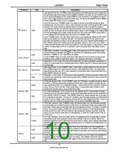
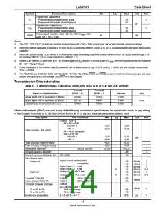
Pin Names
Type
Description
Chip Select/PCM-GCI. The CS/PG input along with the DCLK/S0 input are used to determine
the operating state of the programmable PCM/GCI interface. On power up, the Le58083 Octal
SLAC device will initialize to GCI mode if CS/PG is low and there is no toggling (no high to
low or low to high transitions) of the DCLK/S0 input. The device will initialize to the PCM/MPI
mode if either CS is high or DCLK is toggling.
Once the device is in PCM/MPI mode, it is ready to receive commands through its serial
interface pins, DIO and DCLK. Once a valid command has been sent through the MPI serial
interface, GCI mode cannot be entered unless a hardware reset is asserted or power is
removed from the part. If a valid command has not been sent since the last hardware reset or
power up, then GCI mode can be re-entered (after a delay of one PCM frame) by holding CS/
PG low and keeping DCLK static. While the part is in GCI mode, then CS/PG going high or
DCLK toggling will immediately place the device in PCM/MPI mode.
CS_X/PG_X
Input
In the PCM/MPI mode, the Chip Select input (active Low) enables the device so that control
data can be written to or read from the part. The channels selected for the write or read
operation are enabled by writing 1s to the appropriate bits in the Channel Enable Registers of
the Le58083 Octal SLAC device prior to the command. See EC1, EC2, EC3, EC4. of the
Channel Enable Register and Command 4A/4Bh for more information. If Chip Select is held
Low for 16 rising edges of DCLK, a hardware reset is executed when Chip Select returns
High.
Data Clock. In addition to providing both a data clock input and an S0 GCI address input,
DCLK/S0 acts in conjunction with CS/PG to determine the operational mode of the system
interface, PCM/MPI or GCI. See CS/PG for details.
In the PCM/MPI mode, the Data Clock input shifts data into and out of the microprocessor
interface of the Le58083 Octal SLAC device. The maximum clock rate is 8.192 MHz.
Select Bit 0. In GCI mode, S0 is one of two inputs (S0, S1) that is decoded to determine on
which GCI channel pair a four-channel group of the Le58083 Octal SLAC device transmits and
receives data.
Input
Input
DCLK_X/S0_X
DIO_X/S1_X
Data Input/Output. In the PCM/MPI mode, control data is serially written into and read out of
the Le58083 Octal SLAC device via the DIO pin, most significant bit first. The Data Clock
determines the data rate. DIO is high impedance except when data is being transmitted from
the Le58083 Octal SLAC device.
Select Bit 1. In GCI mode, S1 is the second of two inputs (S0, S1) that is decoded to determine
on which GCI channel pair a four-channel group of the Le58083 Octal SLAC device transmits
and receives data.
Input/Output
Input
PCM Data Receive (A/B). In the PCM/MPI mode, the PCM data is serially received on either
the DRA or DRB port during user-programmed time slots. Data is always received with the
most significant bit first. For compressed signals, 1 byte of data for each channel is received
every 125 µs at the PCLK rate. In the Linear mode, 2 consecutive bytes of data for each
channel are received every 125 µs at the PCLK rate.
GCI Data Downstream. In GCI mode, the B1, B2, Monitor and SC channel data is serially
received, from the individual channels, on the Data Downstream input for all four channels of
the Le58083 Octal SLAC device. The Le58083 Octal SLAC device requires four of the eight
GCI channels for operation. The four GCI Channels, out of the eight possible, are determined
by the S0 and S1 inputs. Data is always received with the most significant bit first. 4 bytes of
data for each GCI channel is received every 125 µs at the 2.048 Mbit/s data rate.
Inputs
Input
DRA/DD, DRB
PCM Data Transmit. In the PCM/MPI mode, the transmit data, from the individual channels,
is sent serially out on either the DXA or DXB port or on both ports during user-programmed
time slots. Data is always transmitted with the most significant bit first. The output is available
every 125 µs and the data is shifted out in 8-bit (16-bit in Linear or PCM Signaling mode)
bursts at the PCLK rate. DXA and DXB are High impedance between time slots, while the
device is in the Inactive mode with no PCM signaling, or while the Cutoff Transmit Path bit
(CTP) is on.
GCI Data Upstream. In the GCI mode, the B1, B2, Monitor and SC channel data is serially
transmitted on the Data Upstream output of the Le58083 Octal SLAC device. Which GCI
channels the device uses is determined by the S0 and S1 inputs. Data is always transmitted
with the most significant bit first. 4 bytes of data for each GCI channel is transmitted every 125
µs at the DCL rate.
Outputs
Output
DXA/DU, DXB
Frame Sync. In the PCM/MPI mode, the Frame Sync (FS) pulse is an 8 kHz signal that
identifies Time Slot 0 and Clock Slot 0 of a system’s PCM frame. The Le58083 Octal SLAC
device references individual time slots with respect to this input, which must be synchronized
to PCLK.
Frame Sync. In GCI mode, the Frame Sync (FSC) pulse is an 8 kHz signal that identifies the
beginning of GCI channel 0 of a system’s GCI frame. The Le58083 Octal SLAC device
references individual GCI channels with respect to this input, which must be synchronized to
DCL.
Input
Input
FS/FSC
10
Zarlink Semiconductor Inc.

 ZARLINK [ ZARLINK SEMICONDUCTOR INC ]